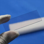
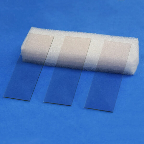
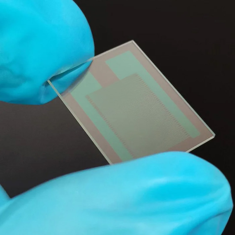
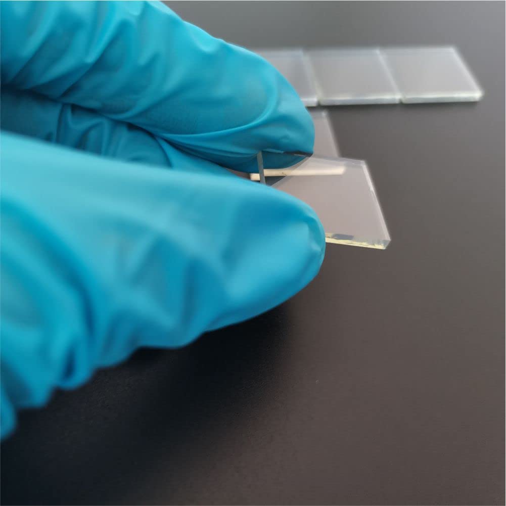
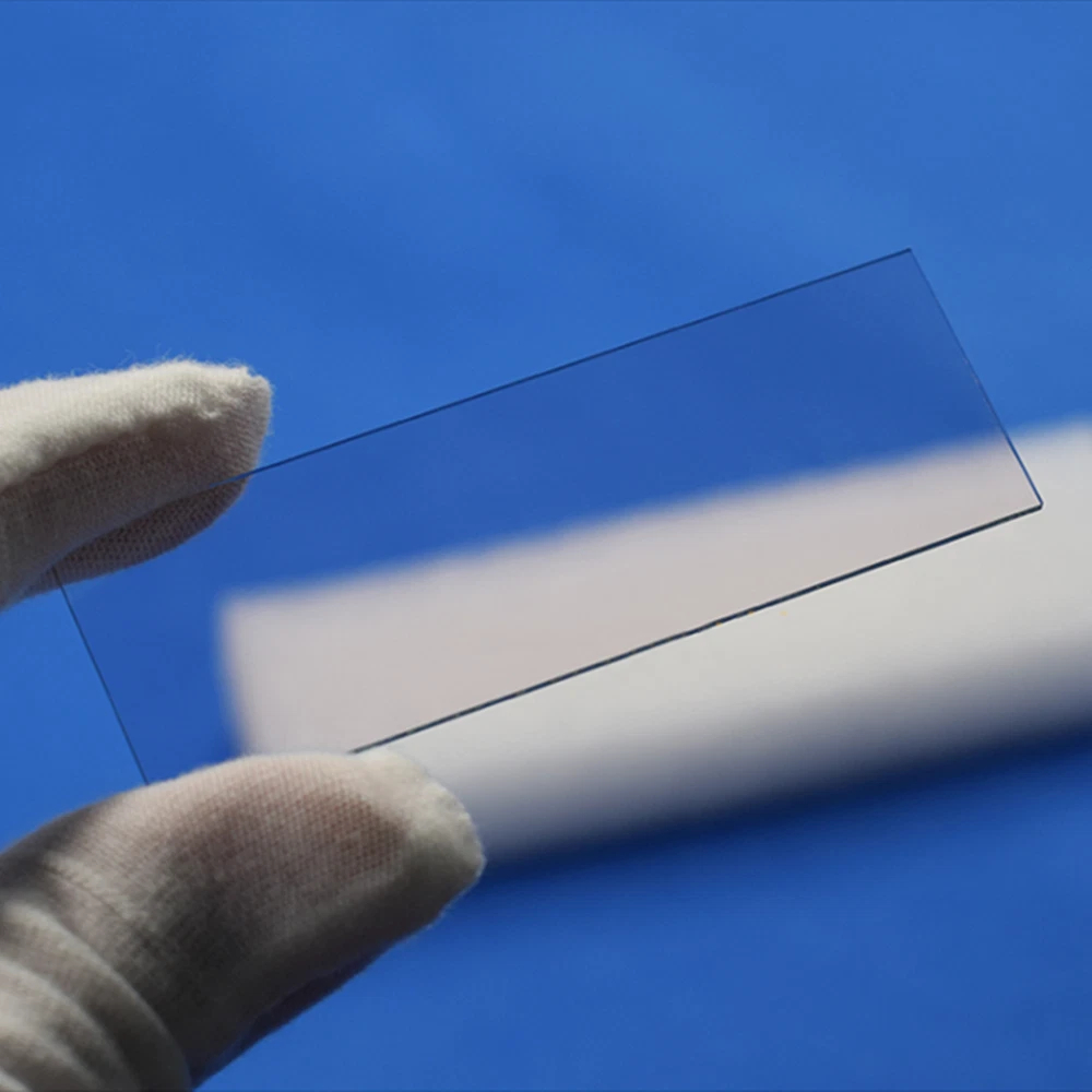
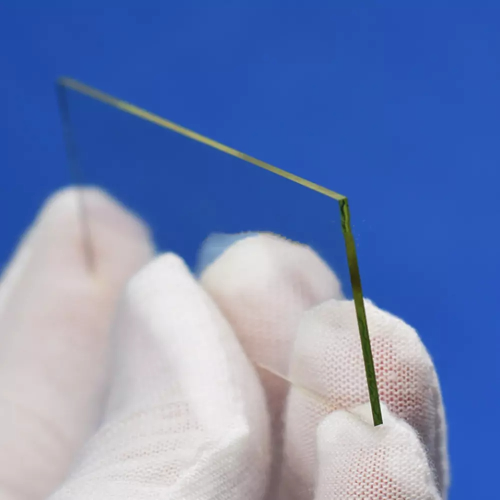
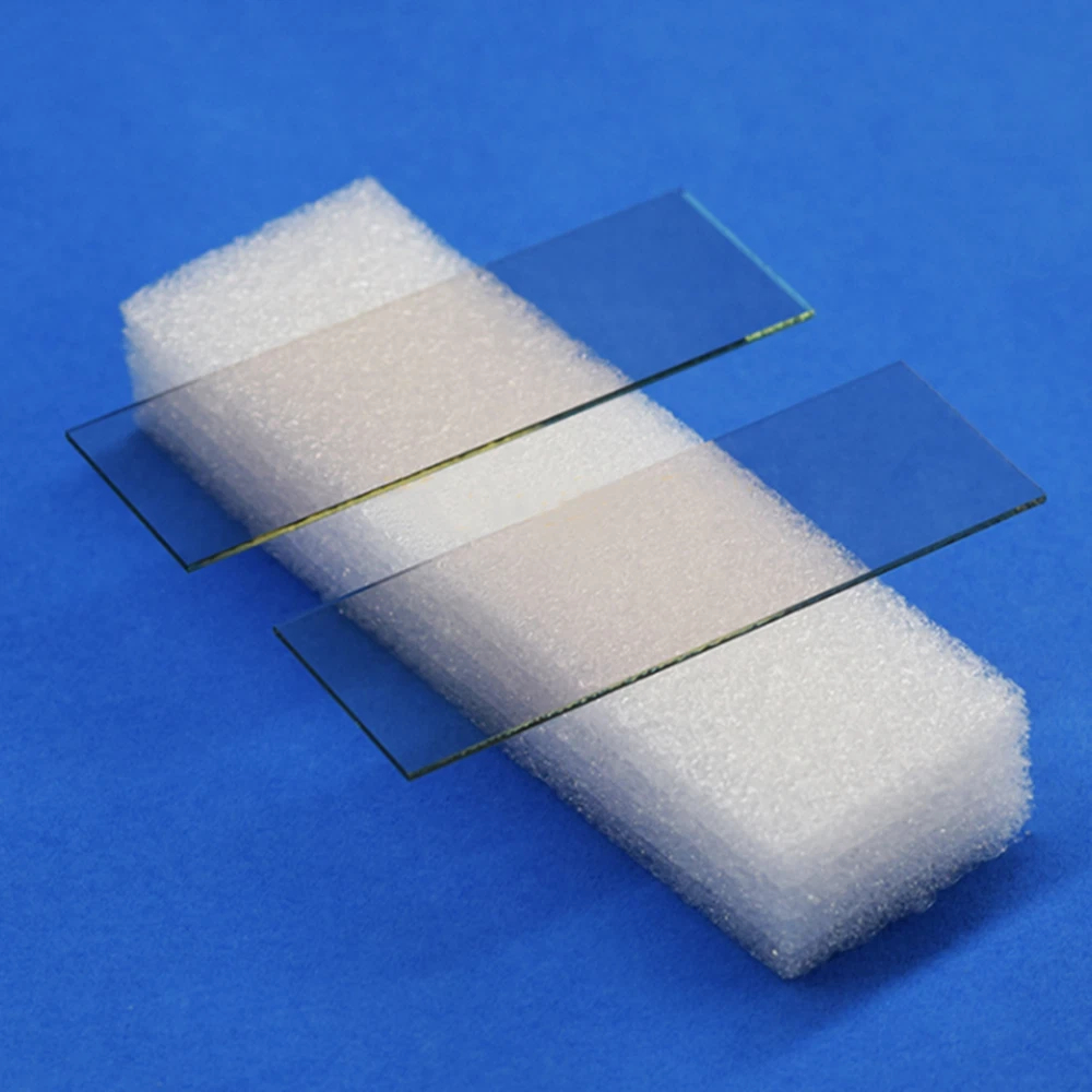
Our conductive glass slides are fabricated using high-purity float or borosilicate glass, then coated with transparent conductive oxides using advanced sputtering or chemical vapor deposition techniques. ITO and FTO films exhibit high optical transparency in the visible range and low sheet resistance, enabling their use in optoelectronic experiments and device prototyping.
ITO / FTO Coated Conductive Glass Slides for Laboratory Applications
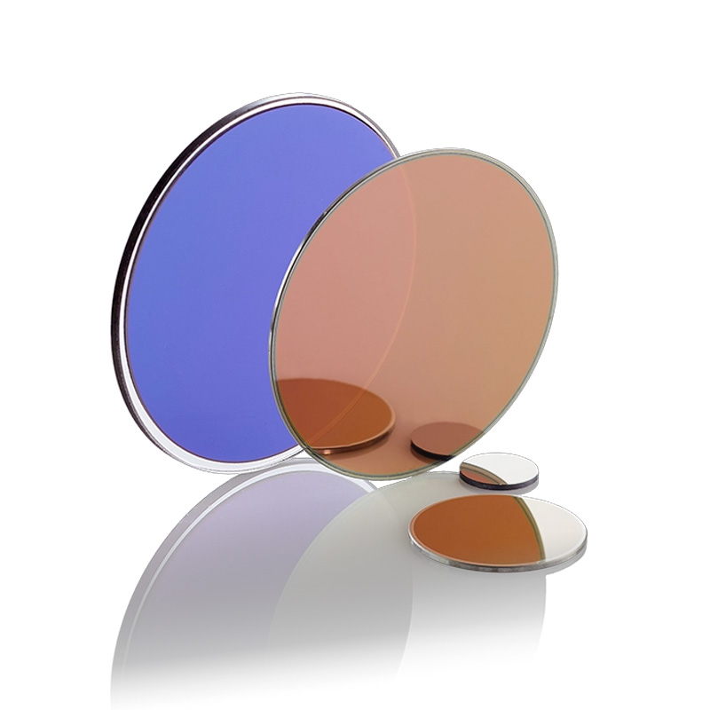
Tihot Optics supplies high-performance ITO (Indium Tin Oxide) and FTO (Fluorine-doped Tin Oxide) coated glass slides engineered for laboratory use in advanced research, electronics, and thin-film device development. These transparent conductive substrates combine excellent optical transmission with consistent electrical conductivity, meeting the demands of modern scientific and technological applications.
Applications & Research Use
These slides are widely used in academic, biomedical, and industrial labs. Typical applications include:
Electrochemical Research: Electrodes for cyclic voltammetry, impedance spectroscopy, fuel cells, and sensors
Photovoltaics: Transparent conductive layer for organic, perovskite, and dye-sensitized solar cells
Microfluidics & Lab-on-a-Chip: Electrode integration for biosensing, impedance flow cytometry, or sample manipulation
OLED/Display Prototyping: Transparent anode layers in display development or touch sensor R&D
Biomedical Devices: Integration into DNA microarrays, wearable electrodes, and diagnostic devices
Ready to start your project? Contact us today for technical consultation, pricing, or to request custom specifications.
Standard Sizes Available
Size (mm)
Thickness (mm)
Notes
25 × 25
1.1 / 2.2
Common for lab-scale PEC & DSSC cells
50 × 50
2.2
Suitable for larger electrode designs
100 × 100
2.2
Ideal for small module prototyping
26 × 76 (microscope slide)
1.1
Compatible with standard lab holders
We support tailor-made specifications based on your application or project requirements:


