

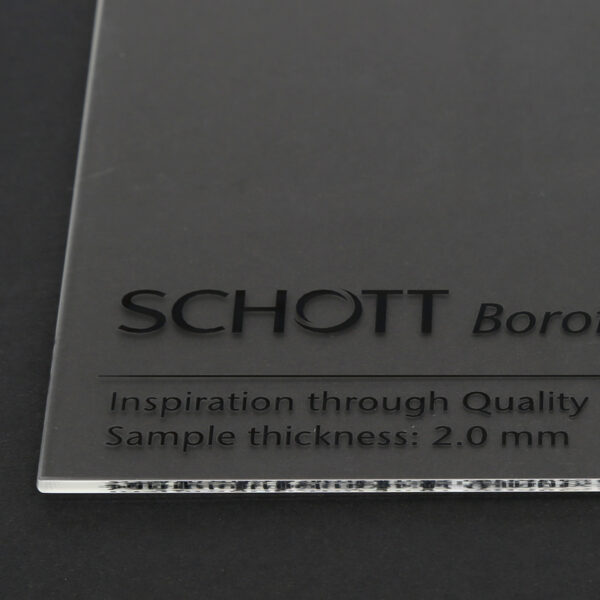
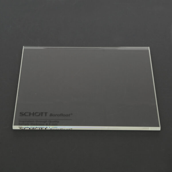
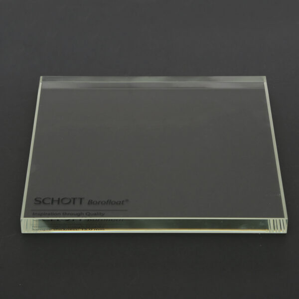
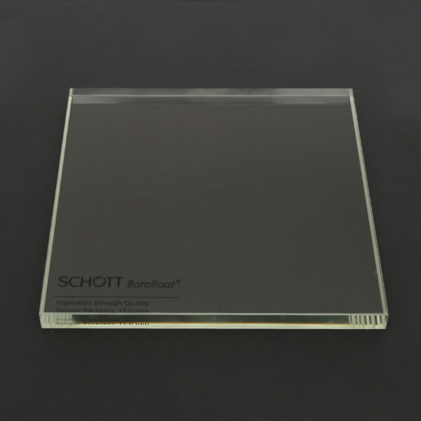
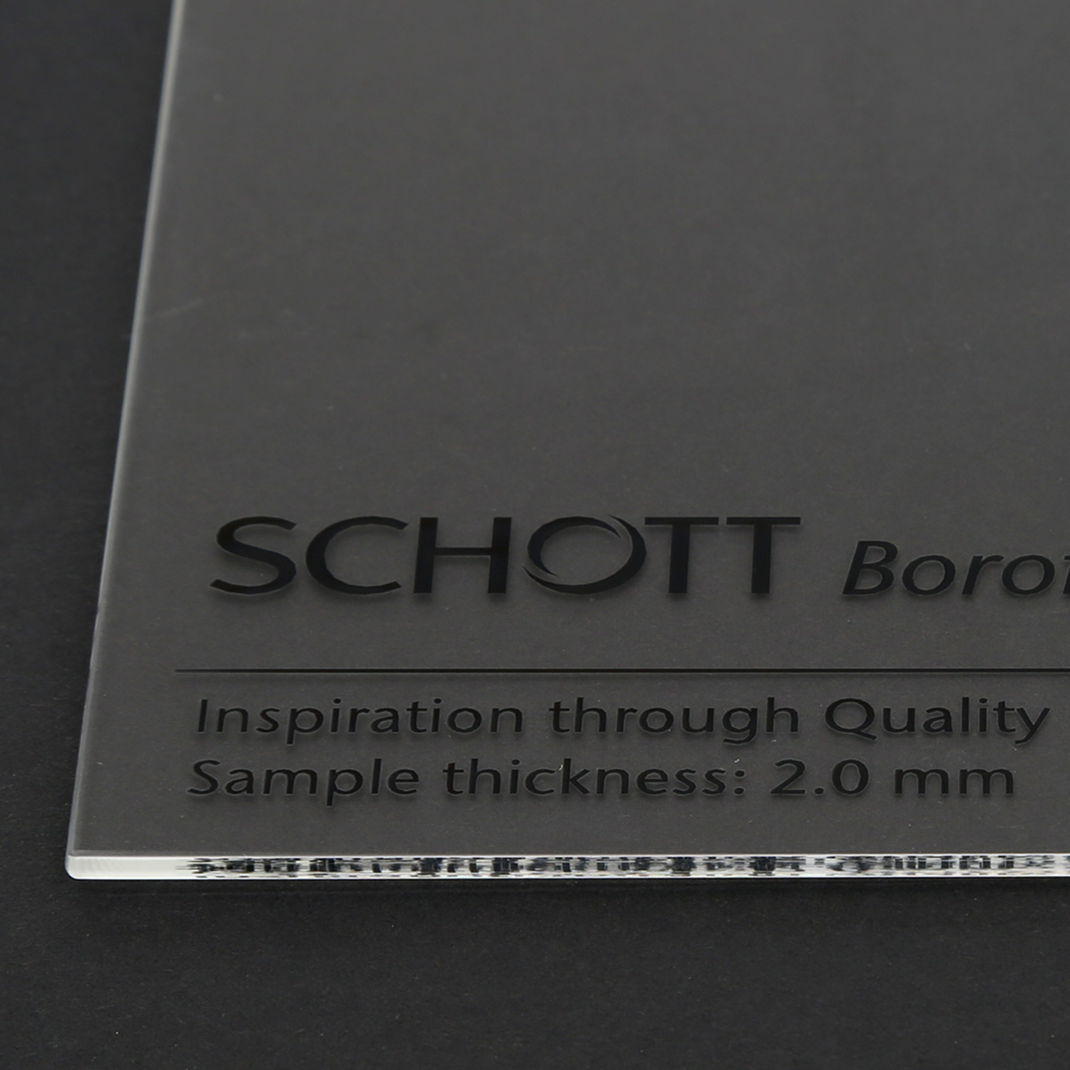
Overview: What is Schott BOROFLOAT® 33 Glass?
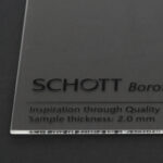
Schott BOROFLOAT® 33 is a premium borosilicate glass manufactured in Germany using a micro-float process. Known for its low thermal expansion, excellent optical transmission, and high chemical resistance, it is widely used in technical and scientific applications.
Compared to conventional borosilicate glass, BOROFLOAT® 33 offers superior surface quality, homogeneity, and workability—making it an ideal choice for high-precision components.
Why Choose BOROFLOAT® 33 for High-Performance Applications?
- Thermal Shock Resistance: With a thermal expansion coefficient of 3.25 × 10⁻⁶/K, it withstands extreme temperature shifts.
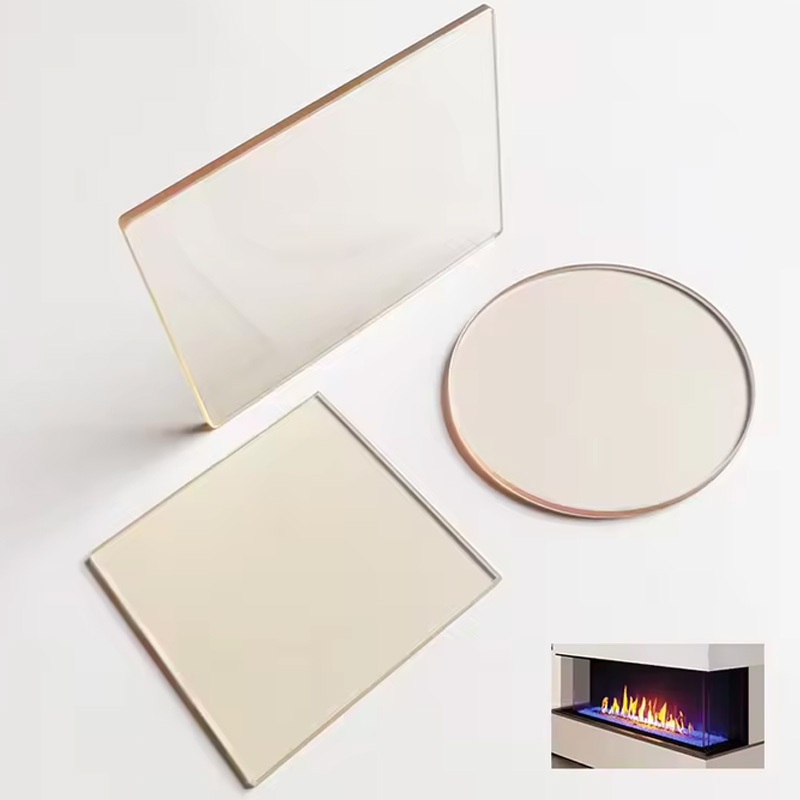
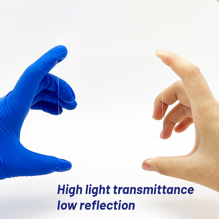
- Optical Quality: Low auto-fluorescence, high transmission in visible and IR spectrum, refractive index ~1.472.
- Mechanical Strength: Knoop Hardness of 480, excellent durability under stress.
- Chemical Durability: Resistant to acids, alkalis, and hydrolytic attack (ISO Class 1).
Your Trusted BOROFLOAT® 33 Supplier and Custom Processor
We are a factory-direct BOROFLOAT® 33 glass supplier offering fully customized solutions for your industrial and scientific needs. Our factory supports:
- Small- and large-batch OEM supply
- Technical consulting for substrate optimization
- International logistics and export documentation
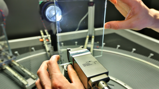
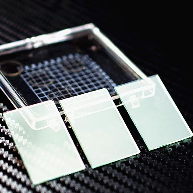
Glass Processing Capabilities for BOROFLOAT® 33
We provide complete in-house fabrication and CNC machining services:
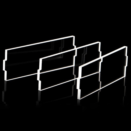
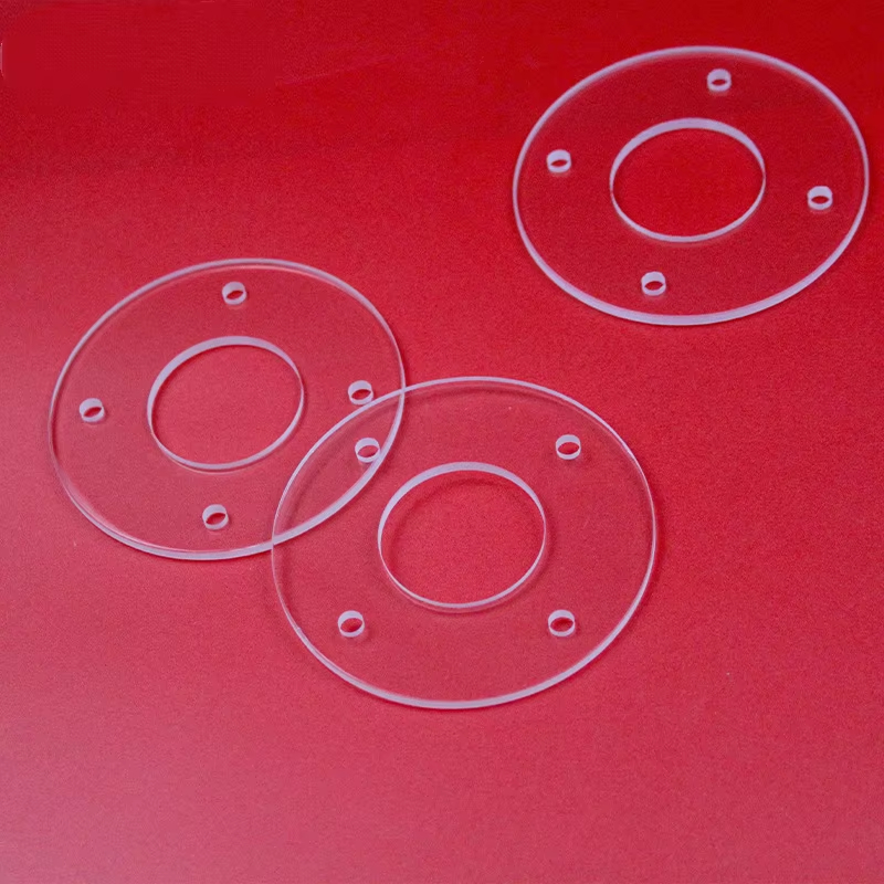
- Precision Cutting: Tolerance up to ±0.01 mm
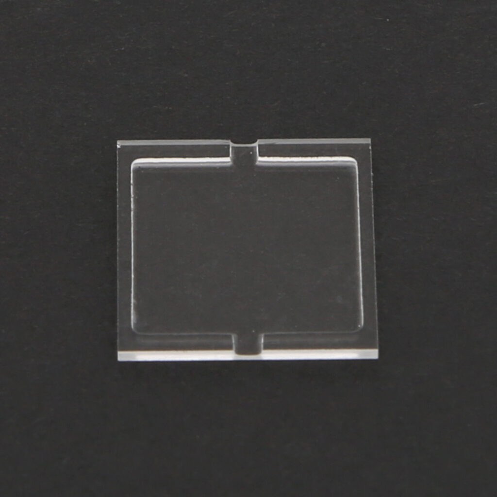
- CNC Milling & Slotting: Complex geometries for optical and MEMS use
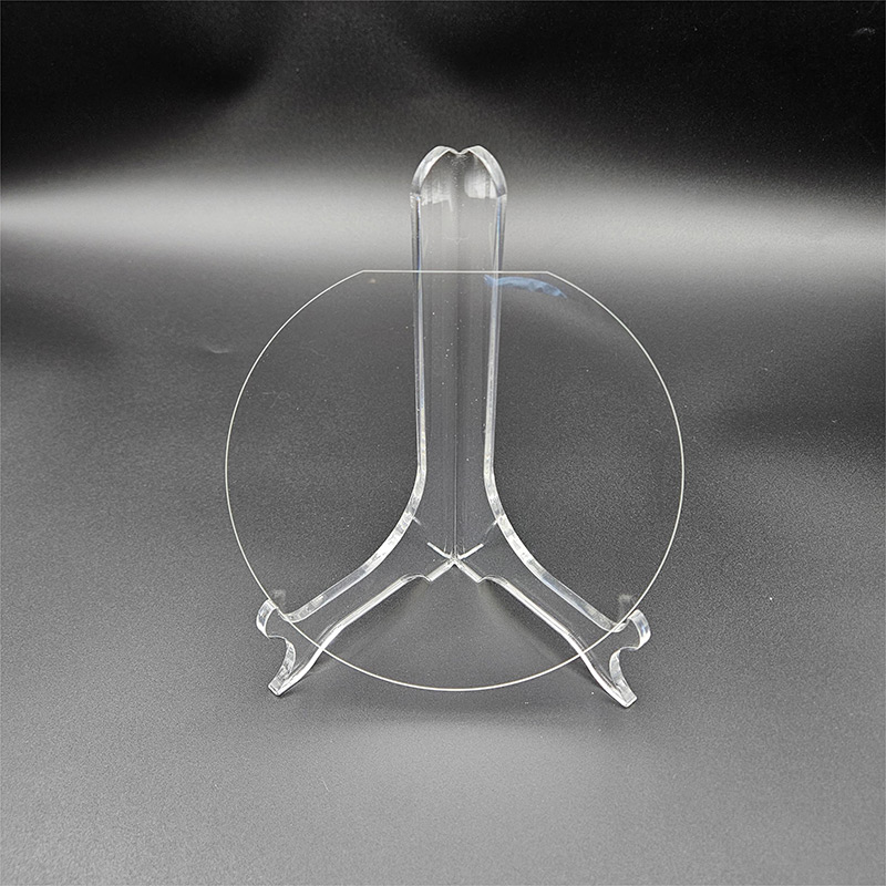
- Edge Polishing: C-edge, D-edge, beveling, and chamfering
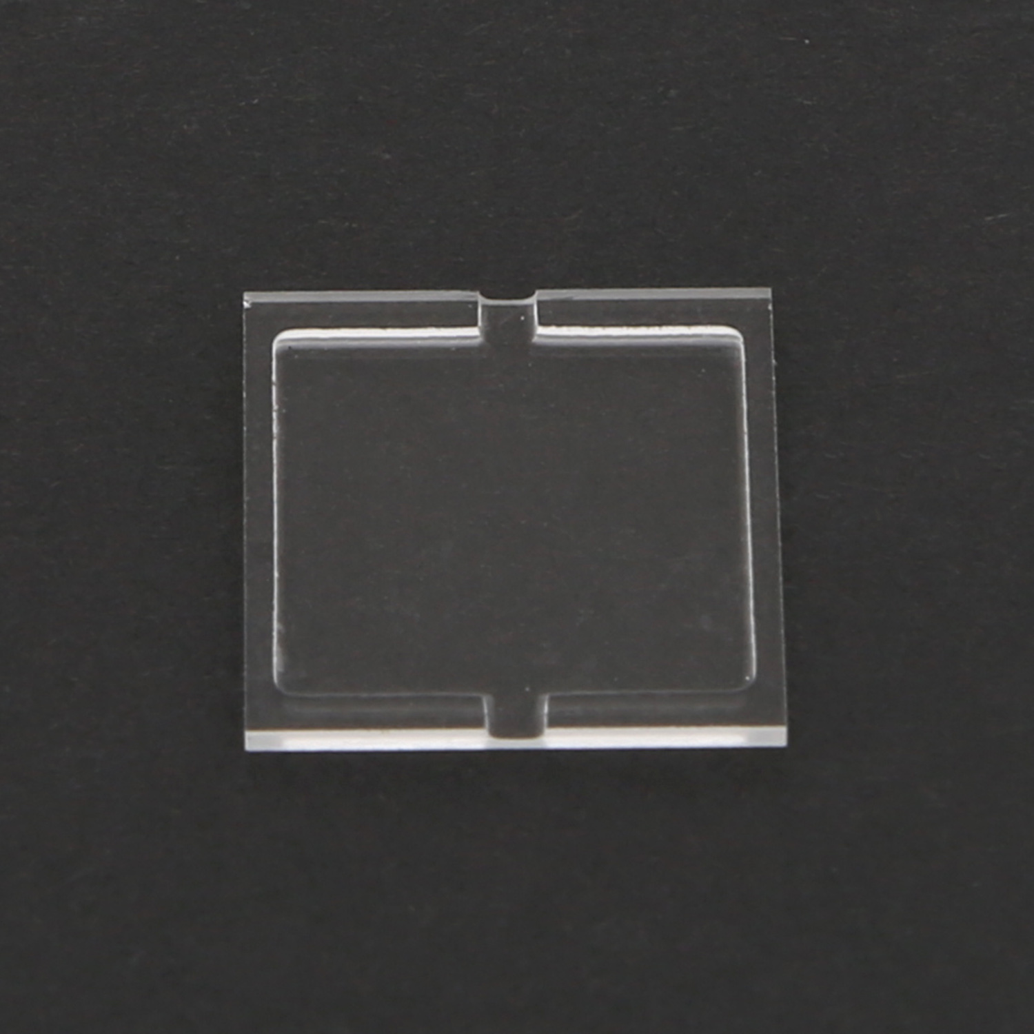
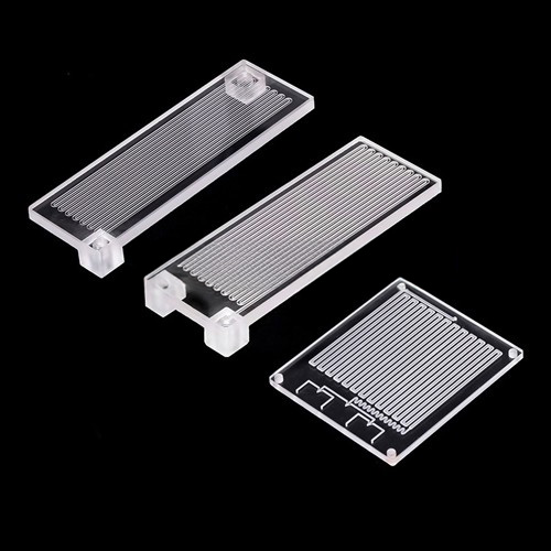
- Drilling & Hole Arrays: For microfluidics or instrumentation
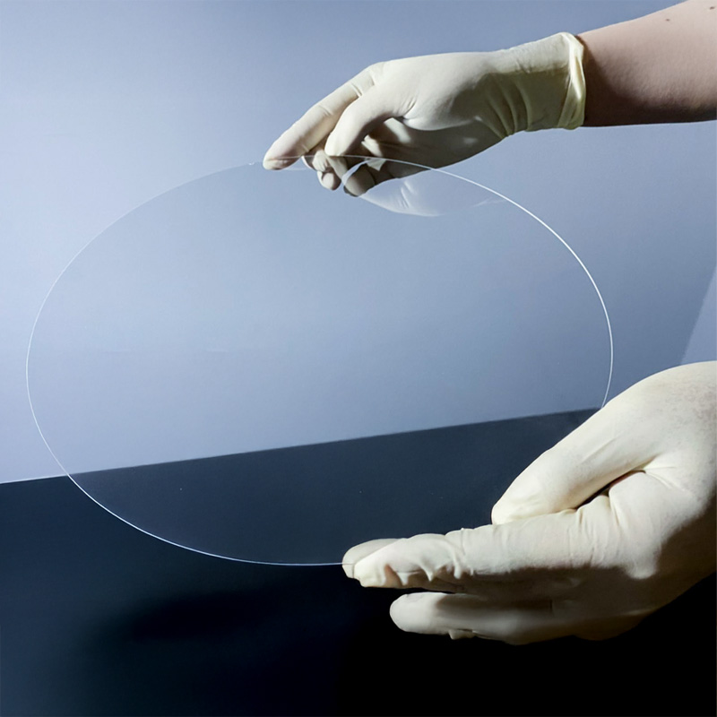
- Surface Finishing: Optical polishing, lapping (Ra ≤ 0.01 µm)
- Coating: Anti-reflective, ITO/FTO, dielectric layers
- Thermal Strengthening: Annealing and thermal tempering available
All fabrication is backed by ISO-aligned quality inspection and CAD/CAM file compatibility (STEP/DXF).
Industries and Applications Served
Optical and Photonics
- Substrates for laser mirrors, beam splitters, filters
- AR-coated windows and optical wafers
Medical and Biotech
- Microfluidic chip carriers
- Diagnostic platforms with optical access
Semiconductor and MEMS
- Thin glass wafers for wafer-level packaging
- Dielectric insulating substrates
Industrial Engineering
- High-temperature viewports, inspection windows
- Transparent shields in laser and cutting systems
Aerospace and Defense
- Lightweight sensor covers and heat shields
- IR-transparent optical domes
Trusted Partner for Universities and Research Laboratories Worldwide
We proudly support universities, research institutes, and national laboratories across the globe with custom glass components tailored for advanced experimentation and scientific innovation.
Whether it’s custom-cut BOROFLOAT® 33 microscope slides, precision-coated optical substrates, or chemically stable microfluidic glass chips, our engineering team works closely with academic clients to deliver:
- Application-specific materials with exact tolerances
- Cleanroom-ready packaging and documentation
- Rapid prototyping for research validation
- Long-term supply stability for extended research programs
The BOROFLOAT®33 glass we process is widely used in spectral devices, biological imaging, laser research and material testing platforms, making us a reliable partner in the global R&D community.
People Also Ask
1. What machining services are available for Schott BOROFLOAT® 33 glass?
We offer a full range of machining services including CNC cutting, drilling, slotting, edge grinding, optical polishing, and surface coating. Thermal tempering and microhole drilling are also available.
2. Can BOROFLOAT® 33 glass be laser cut?
Yes, BOROFLOAT® 33 can be precision laser cut, especially for thin substrates. However, for thicker parts or complex geometries, CNC milling is often preferred to reduce edge chipping.
3. What are the thickness tolerances for custom BOROFLOAT® 33 substrates?
We can achieve thickness tolerances as tight as ±0.01 mm depending on the dimensions and application, especially for optical or semiconductor substrates.
4. Is it possible to drill microholes or channels into BOROFLOAT® 33 for microfluidic or sensor use?
Yes. We support micro-drilling (hole diameters <0.5mm), slotting, and channel etching suitable for microfluidics, MEMS, or sensor applications, all while maintaining structural integrity.
5. Can anti-reflective or conductive coatings be applied to BOROFLOAT® 33?
Absolutely. We offer AR coatings, ITO/FTO conductive layers, and dielectric coatings depending on your optical, electronic, or EMI shielding requirements.
6. What surface finishes are available for BOROFLOAT® 33 glass?
We provide various surface finishes including rough-cut, ground, optically polished (Ra ≤ 0.01 µm), and lapped surfaces, customizable for your intended optical or mechanical usage.
7. Can you provide chamfered or beveled edges for BOROFLOAT® 33 parts?
Yes, we offer edge finishes such as C-edge, D-edge, beveled, and safety chamfering for enhanced handling safety and precision alignment in assemblies.
8.Do you offer small batch or prototype orders?
Absolutely. We support small-batch prototyping, low MOQ orders, and fast turnaround for research institutes, OEM developers, and niche technical applications.