Overview: What is SCHOTT AF32® Wafer?
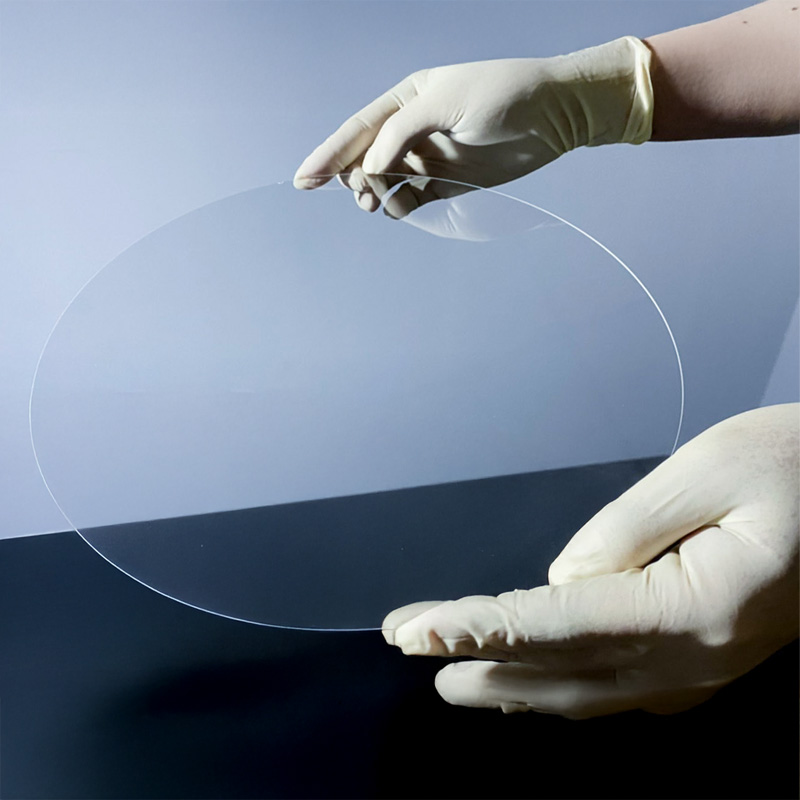
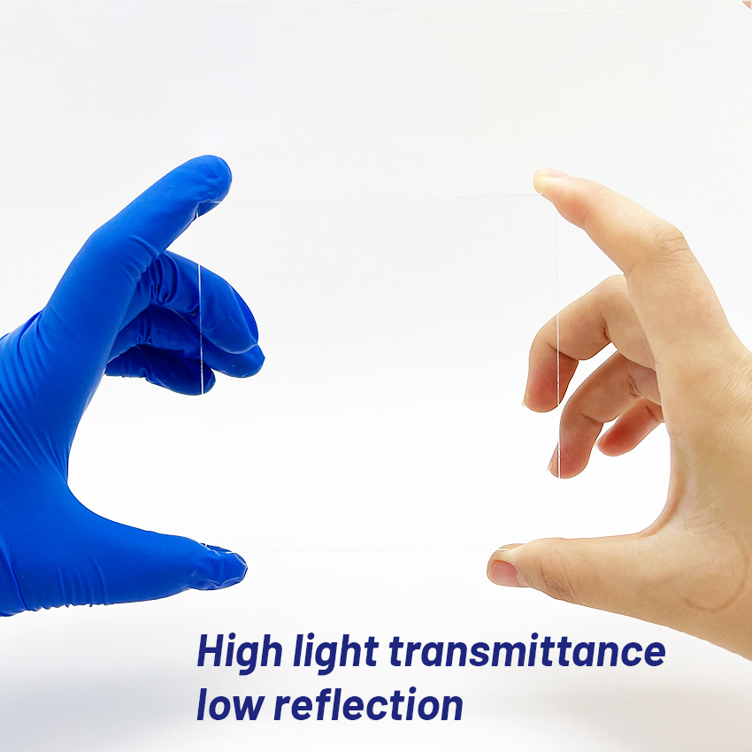
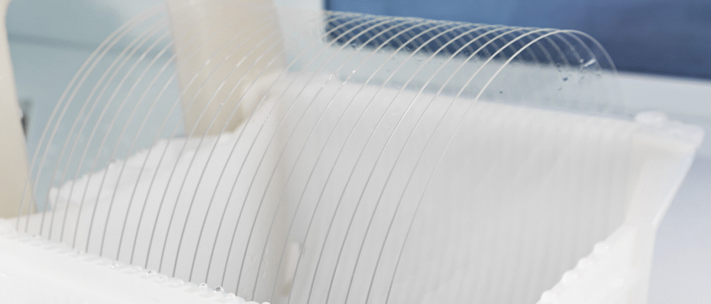
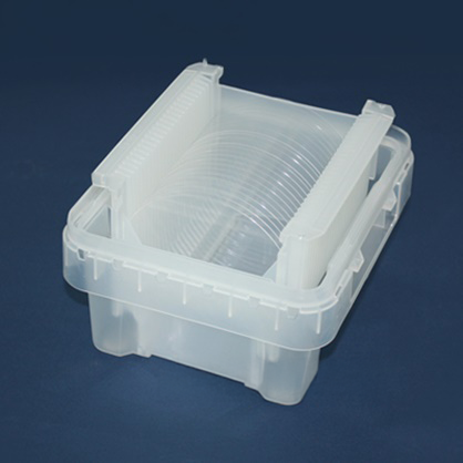
SCHOTT AF32® eco wafer is a premium alkali-free borosilicate glass wafer developed by SCHOTT Germany. Known for its low thermal expansion, excellent surface quality, and compatibility with semiconductor processes, AF32 is widely used in MEMS, microfluidics, and optical device packaging.
As a zero-alkali substrate glass, AF32 offers high dimensional stability and low ionic contamination, making it an ideal base material for photolithography, sensor packaging, and biochips.
Why Choose AF32 Glass Wafers for Advanced Applications?
-
- Alkali-free Composition: No sodium or potassium ions; ideal for semiconductor integration and preventing contamination.
-
- Low Thermal Expansion: CTE of ~3.2 × 10⁻⁶/K, comparable to silicon, ensures dimensional stability.
-
- High Optical Transmission: Exceptional clarity across visible and near-infrared ranges; suitable for optical MEMS.
-
- Excellent Surface Quality: Polished to sub-micron flatness; compatible with cleanroom environments.
-
- Environmentally Friendly: Lead-free, arsenic-free; fully RoHS and REACH compliant.
Your Trusted AF32 Wafer Supplier and Custom Glass Processor

TiHot is a professional AF32 glass wafer supplier and manufacturer offering end-to-end customization services. As a direct factory, we support:
-
- Small-volume prototyping and batch OEM supply
-
- Technical consulting and drawing assistance (DXF/STEP compatible)
-
- Export logistics and international delivery (DHL/FedEx/EXW/FCA/FOB)
We specialize in high-precision AF32 processing for the optical, biomedical, and semiconductor industries.
Glass Processing Capabilities for AF32 Wafer
We provide full in-house CNC and polishing services for AF32 substrates:
-
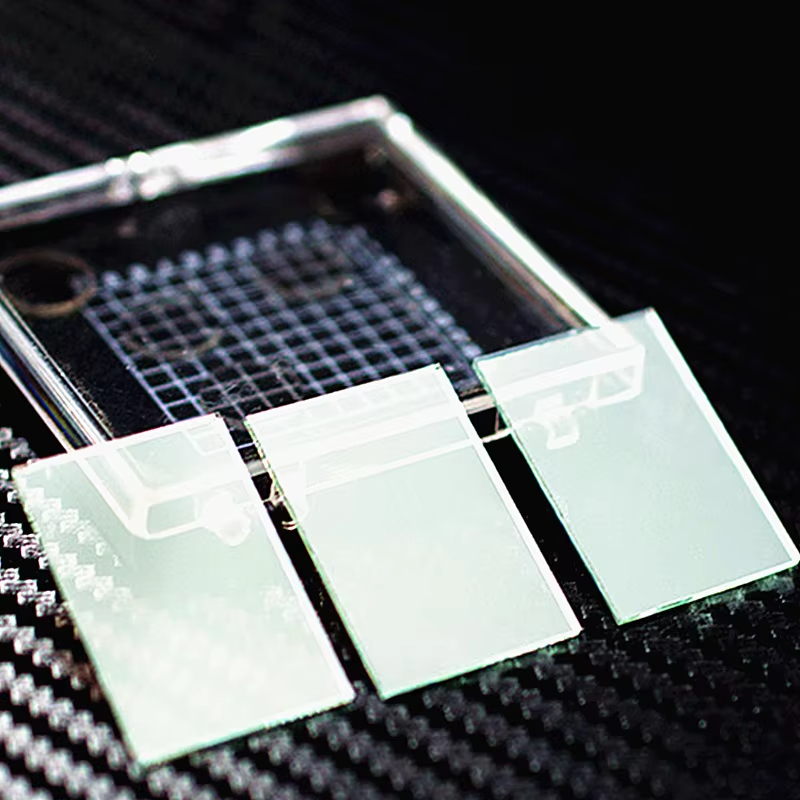
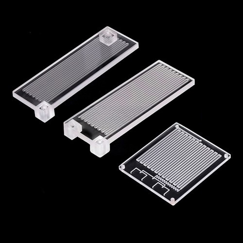
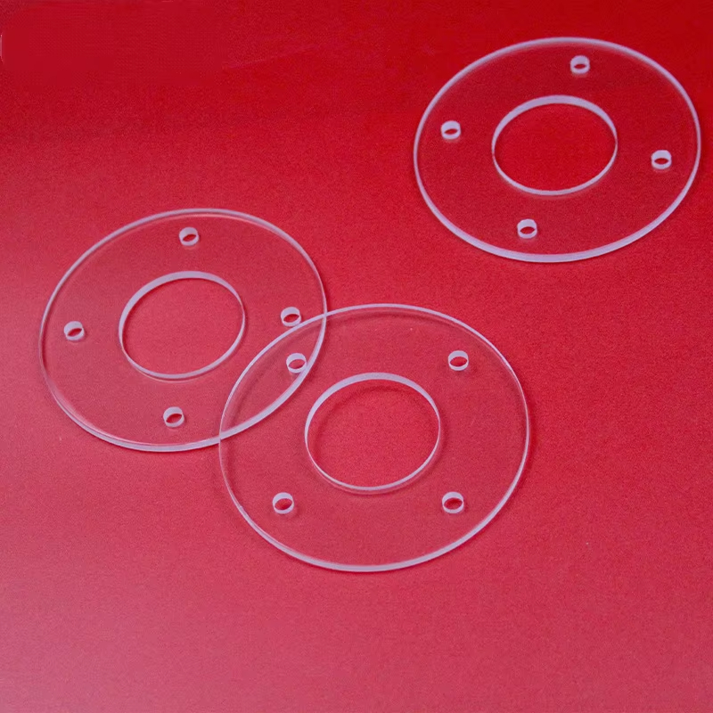
- Precision Dicing & Cutting: ±0.01 mm tolerance, round or square wafers (custom sizes available)
-
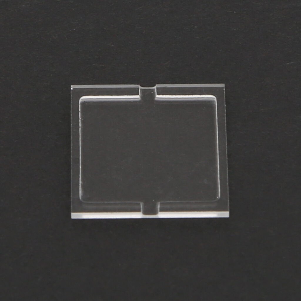
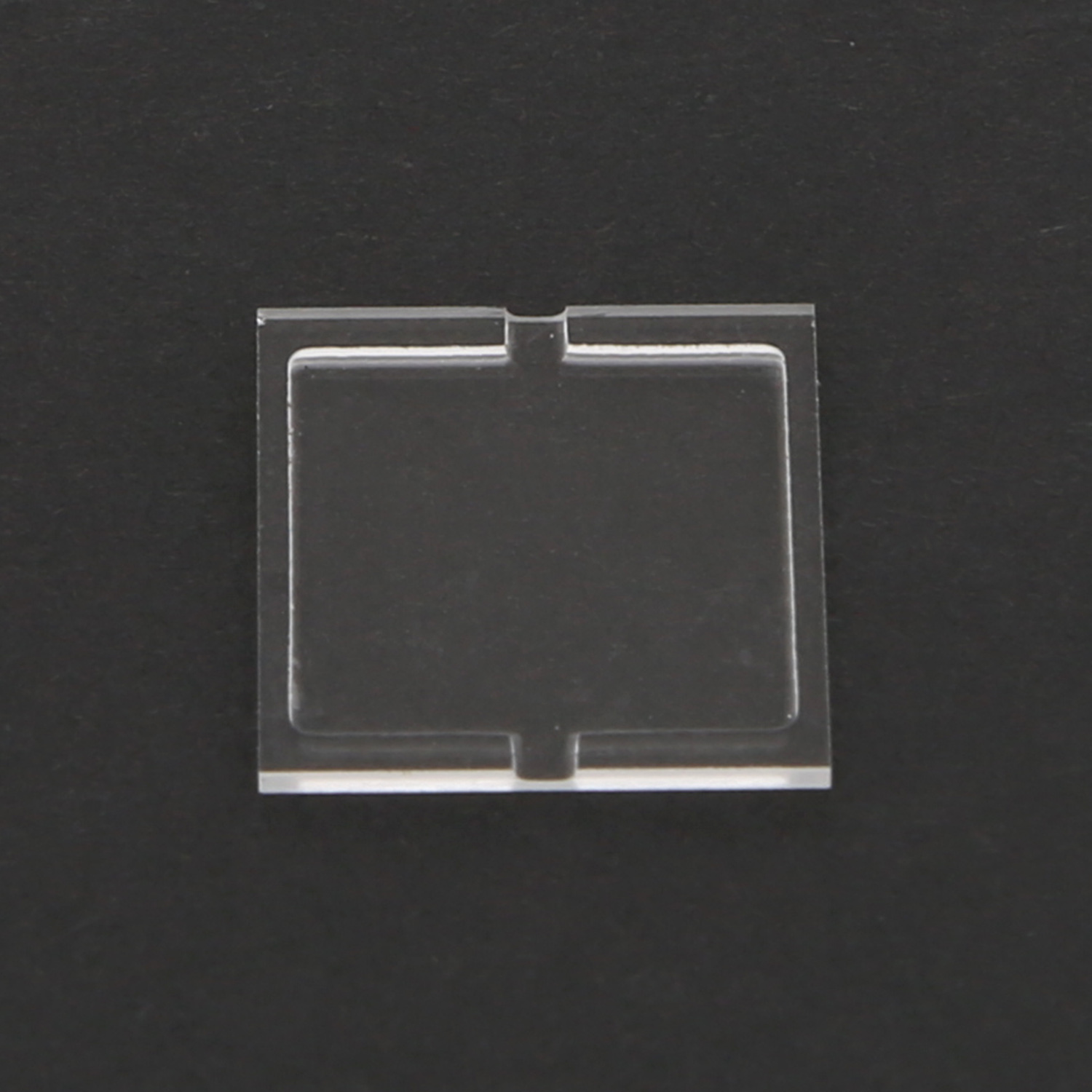
- CNC Slotting & Microchanneling: For MEMS and microfluidic designs
-
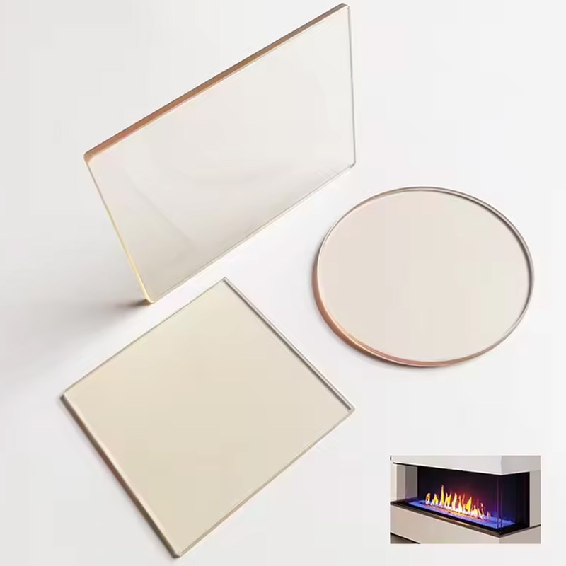
- Edge Finishing: C-edge, D-edge, beveling, chamfering for safety and alignment
-
- Drilling & Microholes: Hole diameters from 0.1 mm; suitable for lab-on-chip systems
-
- Surface Polishing: Ra ≤ 0.01 µm optical polish available
-
- Coating Options: Anti-reflective (AR), ITO/FTO conductive coating, dielectric layers
-
- Thermal Processing: Tempering and annealing available for strength optimization
Industries and Applications Served
-
- Semiconductor and MEMS
-
- Wafer-level packaging
-
- Sensor die substrates
-
- MEMS device covers
-
- Semiconductor and MEMS
-
- Microfluidics and Biotech
-
- Lab-on-a-chip platforms
-
- AF32 microfluidic carriers
-
- Biocompatible glass channels
-
- Microfluidics and Biotech
-
- Optoelectronics
-
- Optical wafers
-
- Transparent substrates for imaging and detection
-
- Filter glass wafers
-
- Optoelectronics
-
- Laser and Photonics
-
- Laser protection windows
-
- Thin optical elements
-
- Calibration substrates
-
- Laser and Photonics
Partner of Choice for Research Institutions and OEM Innovators
We are proud to supply research-grade AF32 glass wafers to universities, R&D labs, and precision engineering firms globally. Whether for:
-
- Prototype development
-
- Microfabrication platforms
-
- Cleanroom-ready optical elements
Our team delivers high-purity AF32 substrates with tailored specifications.
People Also Ask
-
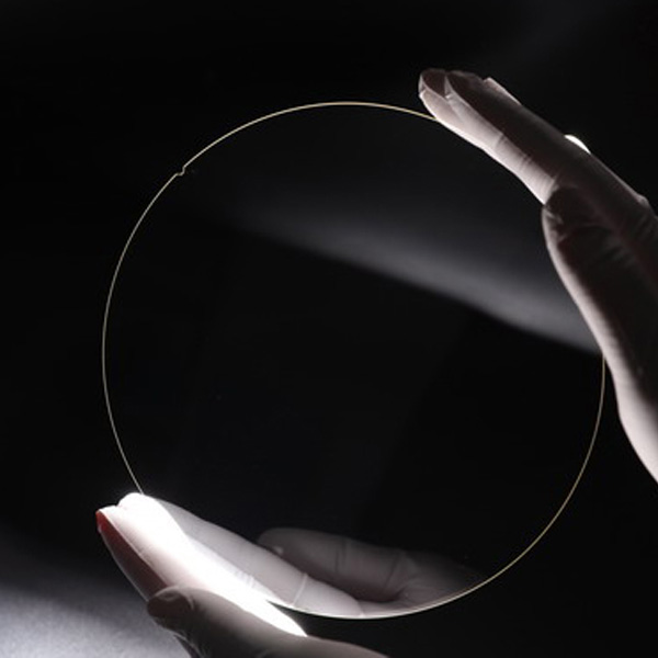
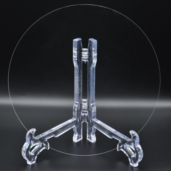
- Can AF32 glass be customized into round wafers or rectangular plates? Yes. We support full customization of shape, diameter (e.g. 4”, 6”), and thickness per your design files.
-
- What is the thickness range available for AF32 wafers? We offer AF32 thickness from 0.1 mm to 1.1 mm, with ultra-thin options for flexible MEMS applications.
-
- Do you support microhole or microchannel drilling on AF32 wafers? Absolutely. Laser drilling and CNC channeling for microfluidic or sensor integration are supported.
-
- What surface finishes are offered for AF32 glass? We provide rough-cut, ground, optical polished (Ra ≤ 0.01 µm), and lapped finishes.
-
- Can you supply small-batch prototype wafers? Yes. We support low MOQ orders and fast turnaround times for research and OEM development.
-
- Is AF32 glass compatible with photolithography and anodic bonding? Yes, its alkali-free and thermally stable characteristics make it ideal for such semiconductor processes.
-
- Do you provide ITO/FTO coating on AF32 glass? We offer high-uniformity conductive coatings like ITO and FTO, compatible with photolithography and deposition.