

What is a Fused Quartz Wafer?
Fused quartz wafer is a high-purity, amorphous silica substrate made by melting natural crystalline quartz (SiO₂) into a glassy, non-crystalline structure. Unlike regular glass wafers, fused quartz offers exceptional thermal stability, chemical inertness, and optical transmission across UV, visible, and infrared wavelengths.
Produced through flame fusion or electric arc melting, fused quartz wafers exhibit ultra-low thermal expansion (~0.55 × 10⁻⁶ /K) and extremely low impurity content, making them indispensable in semiconductors, photonics, and laboratory applications.
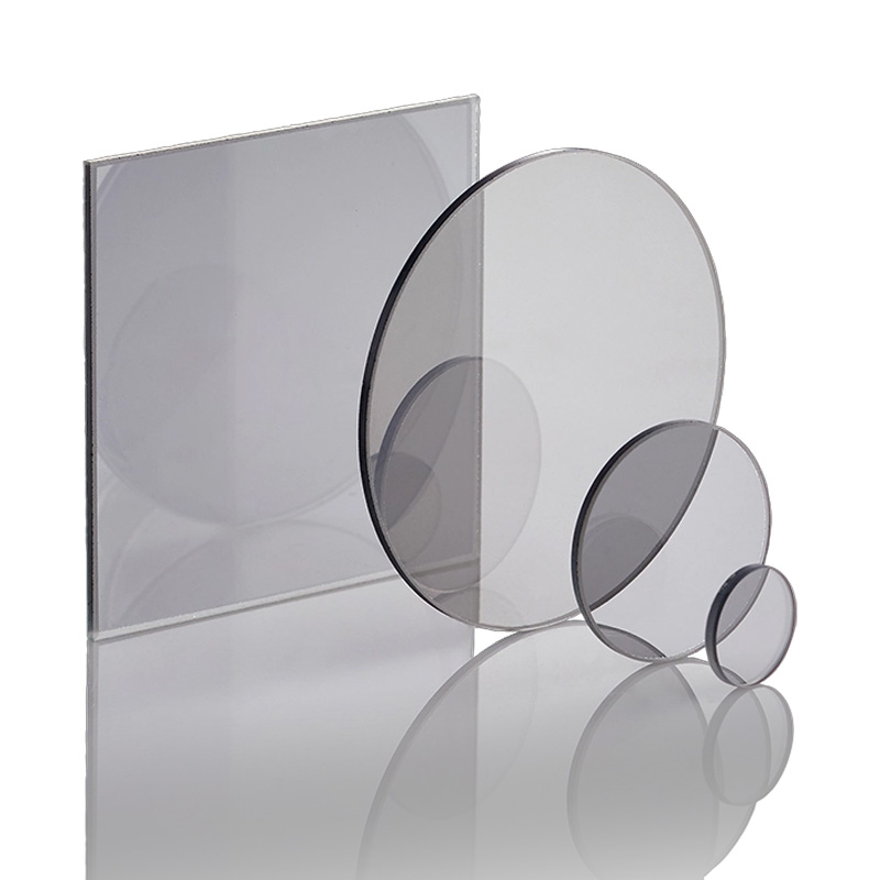
Typical forms include fused quartz wafers, fused silica wafers, and quartz substrates for thin-film deposition, photomask fabrication, and microfluidic device manufacturing.
Why Choose Fused Quartz Wafers for High-Precision Applications?
- High Purity SiO₂ (>99.99%): Guarantees minimal contamination—ideal for IC and optical coating processes.
- Thermal Stability: Withstands continuous temperatures up to 1100°C, short-term exposure to 1200°C.
- Ultra-Low Expansion: CTE ≈ 0.55 × 10⁻⁶ /K ensures dimensional stability during thermal cycling.
- Broad Optical Transmission: 200–2500 nm transmission range, covering UV-VIS-IR applications.
- Chemical Resistance: Excellent durability against most acids, solvents, and plasma etchants.
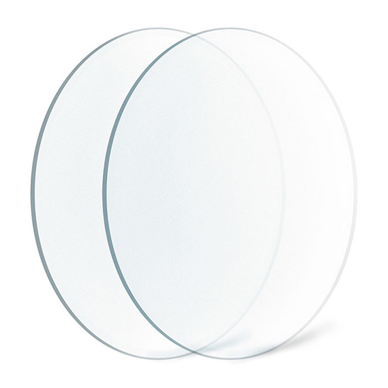
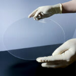
- Surface Quality: Ra < 0.5 nm available for optical-grade surfaces and thin-film bonding.
Your Trusted Fused Quartz Wafer Supplier and Custom Processor
TIHOTOPTICS specializes in the custom fabrication and processing of fused quartz wafers and discs, offering precision substrates for electronics, photonics, optics, and laboratory research.
As a direct manufacturer, we support both OEM production and small-batch prototyping, with fully traceable material certification and international export capability.
Our services include:
- CNC precision machining & polishing (Ra ≤ 0.01 µm)
- Laser cutting and drilling for micro-scale applications
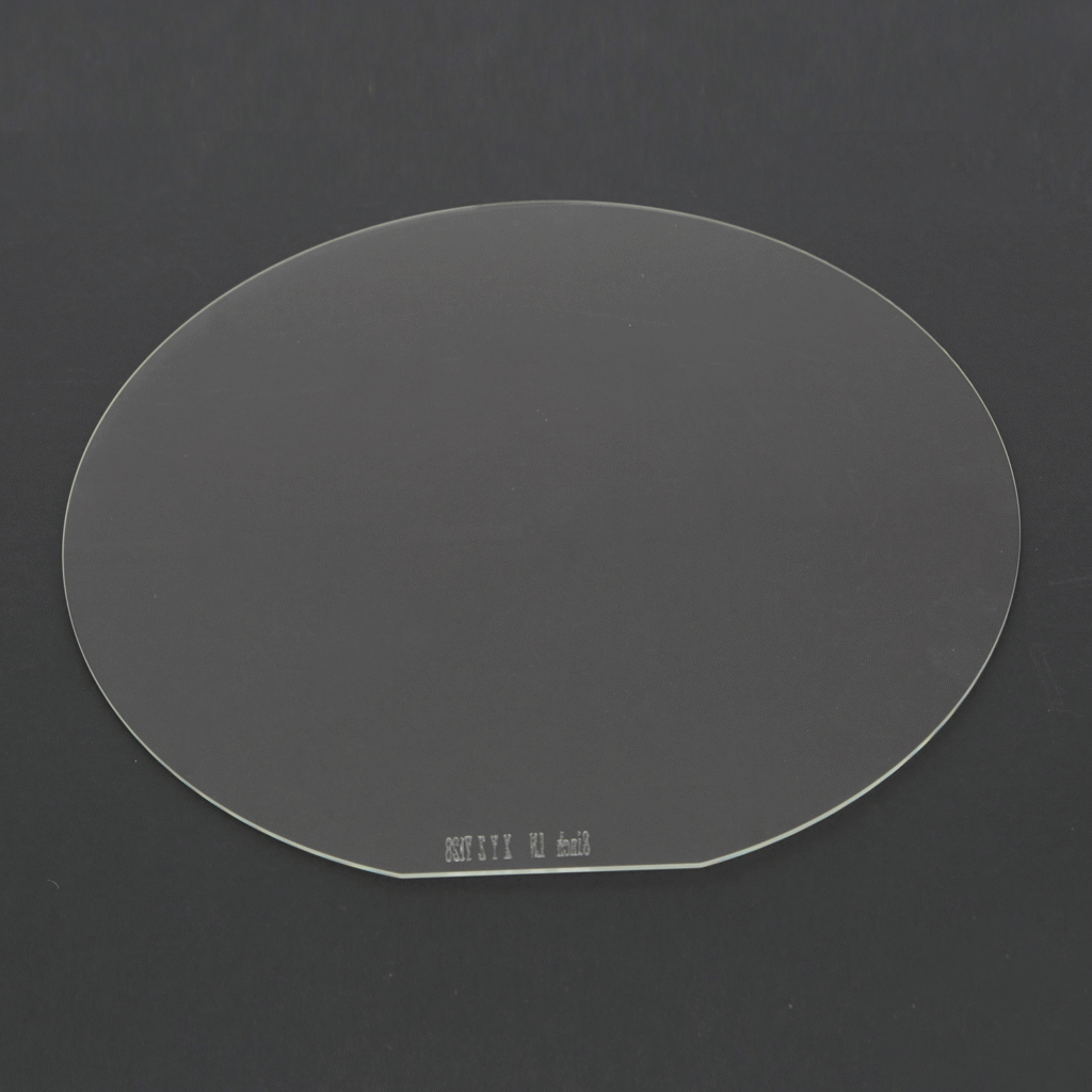
- Custom wafer sizing up to 300 mm diameter
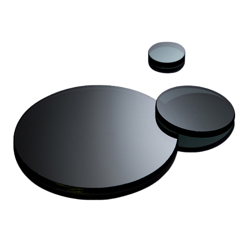
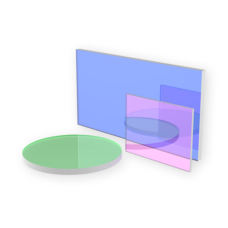
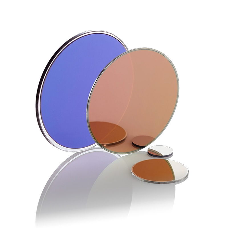
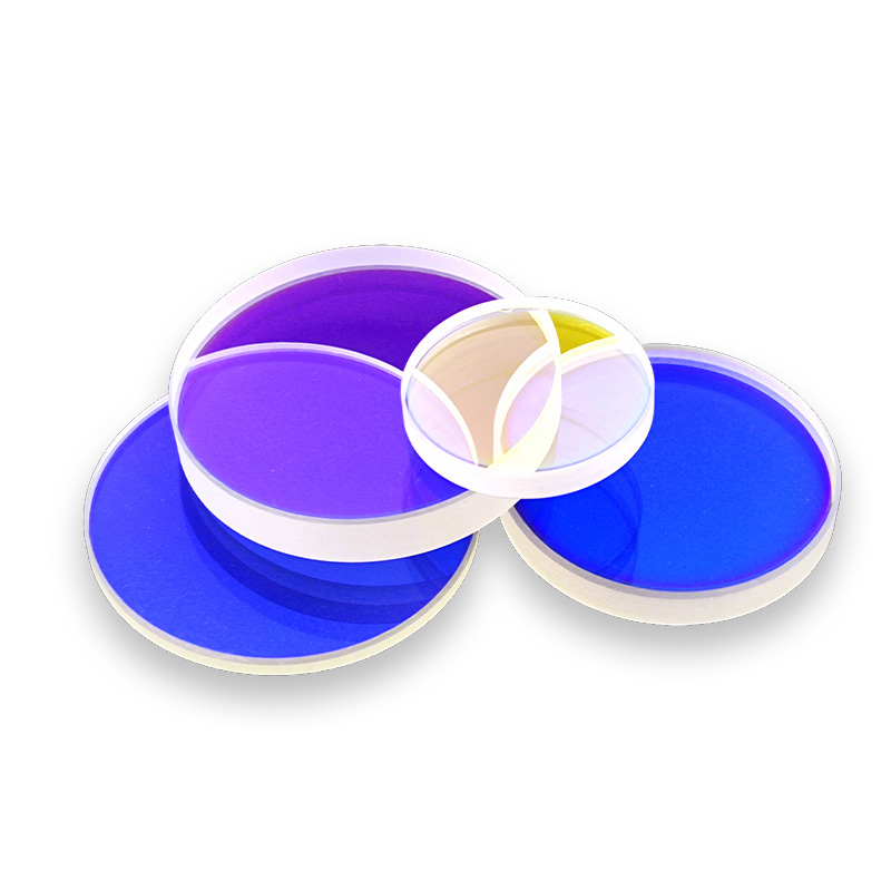
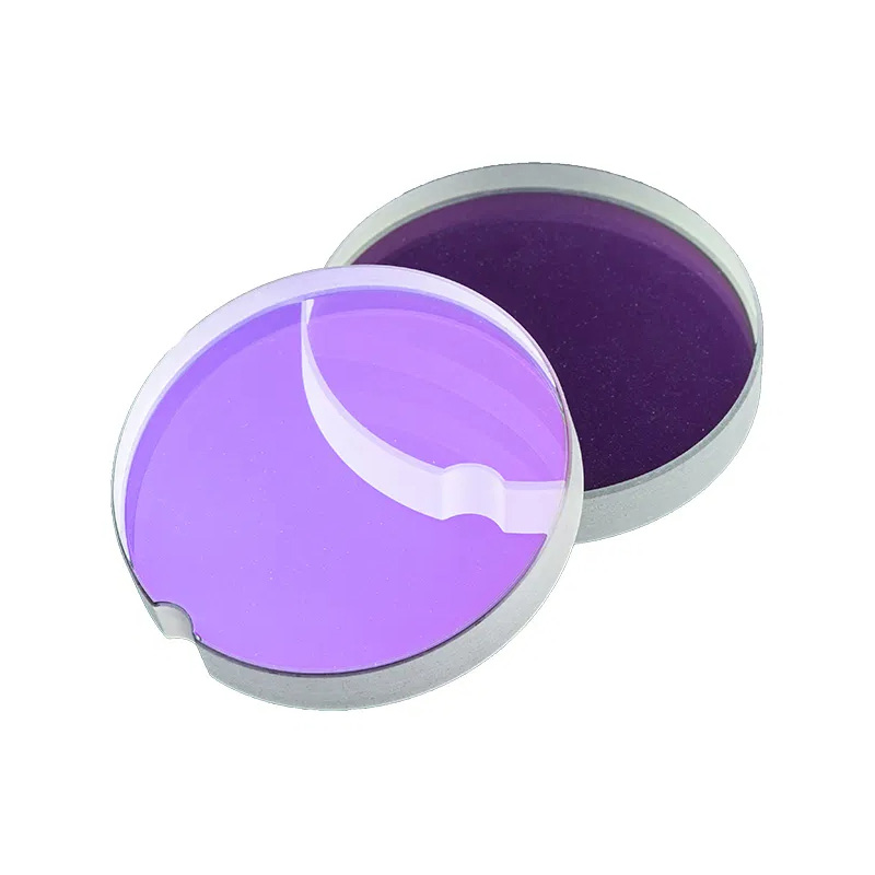
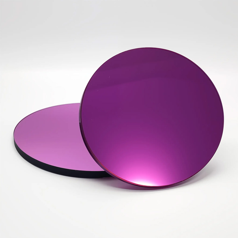
- Coating options: ITO, AR, dielectric, and metallic thin films
Fused Quartz Wafer Processing Capabilities
At TiHot, every fused quartz wafer is produced under ISO quality standards, ensuring superior flatness, low TTV (Total Thickness Variation), and cleanroom-grade packaging.
| Process Type | Specification & Capability |
|---|---|
| Precision Cutting | ±0.01 mm tolerance, any shape (round, square, or custom) |
| CNC Slotting & Dicing | MEMS, optical window, and photomask applications |
| Edge Finishing | C-edge, D-edge, beveled, or chamfered for handling safety |
| Surface Polishing | Optical or lapping finish (Ra ≤ 0.01 µm) |
| Drilling & Microchanneling | Holes ≥ 0.1 mm, precision laser machining |
| Coating Services | ITO, dielectric, and AR coatings upon request |
All wafers undergo optical flatness and surface roughness inspection, ensuring repeatable performance for high-end optical and electronic use.
Industries and Applications Served
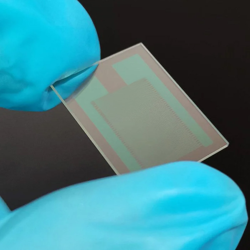
Semiconductor and Microelectronics
- Photolithography masks and optical aligners
- Wafer carriers and high-temperature process windows
- Thin-film deposition and PECVD substrates
Optics and Photonics
- UV/VIS/IR optical windows
- Beam splitters and calibration plates
- Precision metrology and laser optics
Microfluidics and Biomedical Research
- Transparent microfluidic chips
- Bio-imaging and diagnostic substrates
- Chemical analysis cells and reactor platforms
Aerospace and Energy
- High-temperature viewports
- Plasma reactor components
- Optical sensors for harsh environments
Supporting Research and Innovation
TiHot supports universities, laboratories, and advanced R&D facilities with rapid prototype support and engineering collaboration.
We specialize in:
- Ultra-thin quartz wafers for optical MEMS
- Double-side polished wafers for bonding or lithography
- Laser-structured quartz chips for bio and chemical sensors
People Also Ask About Fused Quartz Wafers
1. What is the difference between fused quartz and fused silica?
Both are composed of SiO₂, but fused silica is made from synthetic precursors (ultra-high purity), while fused quartz comes from natural quartz crystals. Fused silica generally has fewer impurities and slightly higher UV transmission.
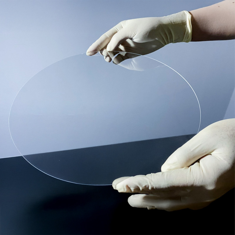
2. What thicknesses are available for fused quartz wafers?
We offer standard thicknesses from 0.3 mm to 3.0 mm, with custom thicknesses up to 10 mm upon request.
3. Can fused quartz wafers withstand high temperatures?
Yes. Fused quartz maintains structural stability up to 1100°C and short-term exposure to 1200°C, making it suitable for furnace and plasma environments.
4. Is fused quartz transparent to UV and IR light?
Yes, it transmits wavelengths from 200 nm (UV) to 2500 nm (IR), ideal for spectroscopy, photolithography, and optical testing.
5. Do you offer coating on quartz wafers?
Yes. We provide ITO, gold, dielectric, and anti-reflective coatings
6. Can you machine micro-holes or channels on quartz wafers?
Yes. Using CNC and laser micromachining, we achieve feature sizes down to 100 µm for microfluidic and MEMS applications.
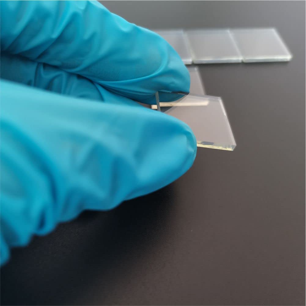
7. Are quartz wafers available in round and square formats?
Absolutely. Standard sizes include 2″, 4″, 6″, 8″, and custom square up to 300×300 mm.、