Glass Etching Processing

What is Glass Etching Processing?

Glass etching processing is a precision microfabrication technique that removes glass material to create patterns, channels, and structures on glass substrates. This process enables manufacturing of high-precision components for semiconductor packaging, microfluidics, MEMS devices, and optical applications where traditional machining cannot achieve the required accuracy.

Our etched glass substrate solutions deliver dimensional tolerances as tight as ±50μm with surface roughness under 0.02μm Ra, meeting demanding specifications across industries from LED packaging to biomedical devices.

Custom Glass Etching Processing

glass Etching Processing

Material Compatibility

Borosilicate glass

fused silica

soda-lime glass

specialty glasses including Gorilla Glass, D263, and AF32.

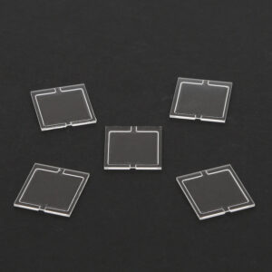
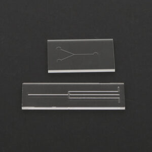
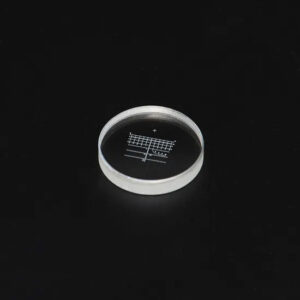
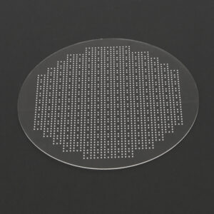
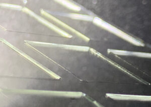
Microchannel Glass Etching Expertise

Channels from 5μm to 5000μm width with depths from 1μm to 500μm. Aspect ratios up to 20:1 with rectangular, trapezoidal, or rounded cross-sectional profiles. Integrated mixing chambers, flow restrictions, and sensor pockets available.

Precision Glass Etching Capabilities

ItemSpecificationRemarks
Alignment Accuracy
Alignment mark size±80 μmCircular drilled mark
Alignment mark tolerance±50 μmIncluding diagonal position
Alignment mark to edge±100 μm 
Cell / Cavity Dimensions
Cell position tolerance±170 μm 
Cell size tolerance±170 μm 
Cavity depth tolerance±50 μm 
Surface Quality
Surface roughness< 0.02 μm Ra 
Glass Substrate Specifications
Max glass panel size920 × 730 mm 
Thickness range0.035 – 1.1 mmStandard: 0.5 / 0.55 / 0.7 / 1.1 mm

Industry Applications

LED Packaging Glass Cover

Precision cavity formation for LED dies with anti-reflection surface texturing and thermal expansion matching. Applications include automotive headlights, display backlights, and high-power industrial lighting systems.

Microfluidic Glass Chip Etching

Complex channel networks from 1μm to 1000μm width with aspect ratios up to 10:1. Serves biomedical diagnostics, drug discovery platforms, and point-of-care testing devices with 3D channel architectures and integrated port features.

Optical Glass Etching

Diffraction gratings, waveguide formation, micro-lens arrays, and integrated photonic circuits with low optical loss surfaces and precise refractive index control for AR/VR and telecommunications applications.

MEMS Glass Substrate Etching

High-precision components for pressure sensors, accelerometers, optical MEMS switches, and biomedical implantable devices requiring tight dimensional tolerances and long-term stability.

Contact Us

Ready to discuss your precision glass etching requirements?

Contact our engineering team for technical consultation, rapid quotation within 24 hours, and sample processing evaluation.

Contact Us Now

*We respect your confidentiality and all information are protected.