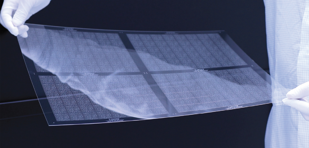
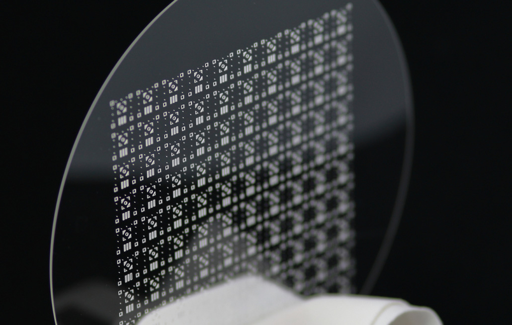
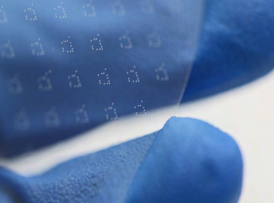
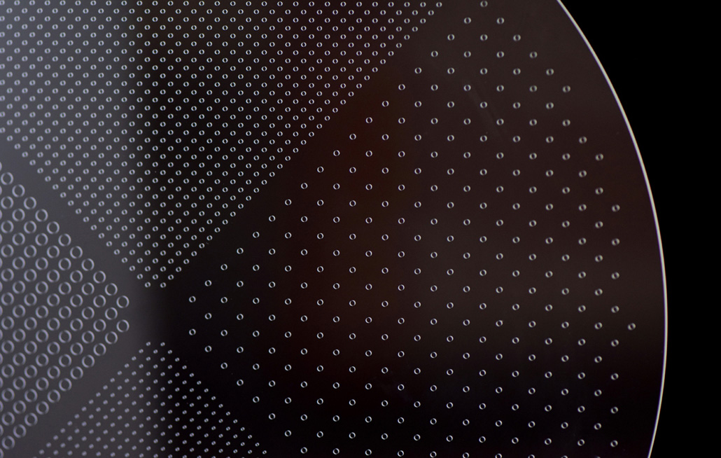
TIHOTOPTICS offers advanced through-glass via (TGV) solutions combining laser drilling and chemical etching techniques. Our hybrid approach enables precise, clean, and high-aspect-ratio vias in glass substrates for MEMS, photonics, and advanced packaging applications.
A Through-Glass Via (TGV) is a micro-scale hole or channel that passes through a glass substrate, enabling vertical electrical, optical, or fluidic interconnections. Unlike traditional through-silicon vias (TSV), glass materials offer superior insulation and dimensional stability, making them ideal for next-generation interconnect technologies.
Glass, which lacks free-moving charges, exhibits excellent dielectric properties and has a thermal expansion coefficient closely matched to silicon. By replacing silicon with glass in TGV structures, the problem of poor insulation often encountered in TSV processes can be effectively avoided. Moreover, TGV fabrication eliminates the need for additional insulating layers, simplifying the process and reducing manufacturing costs.
The core of TGV technology lies in the precise and reliable deep via formation within glass substrates. Thanks to its outstanding electrical insulation, chemical stability, and process compatibility, TGV is recognized as a key enabling technology for next-generation 3D integration.
With these advantages, TGV and related technologies show great potential in a wide range of fields, including optical communications, RF and microwave devices, MEMS, microfluidic systems, and advanced 3D packaging.
Contact Us Now
*We respect your confidentiality and all information are protected.