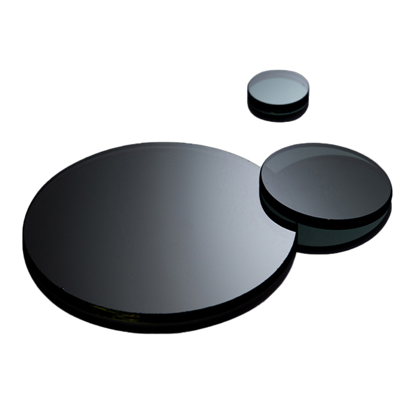
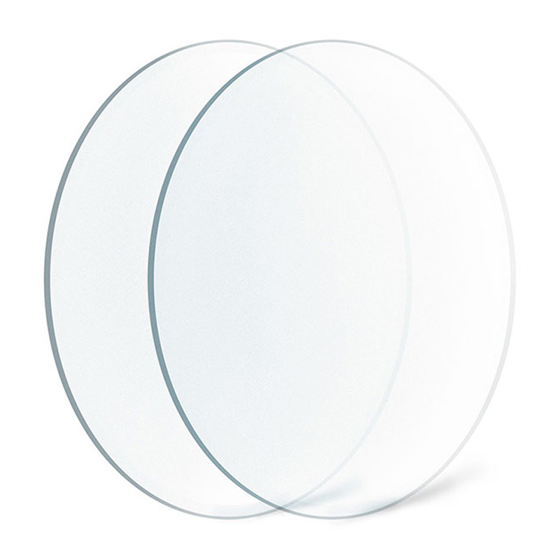
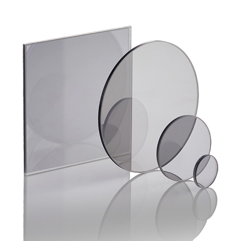
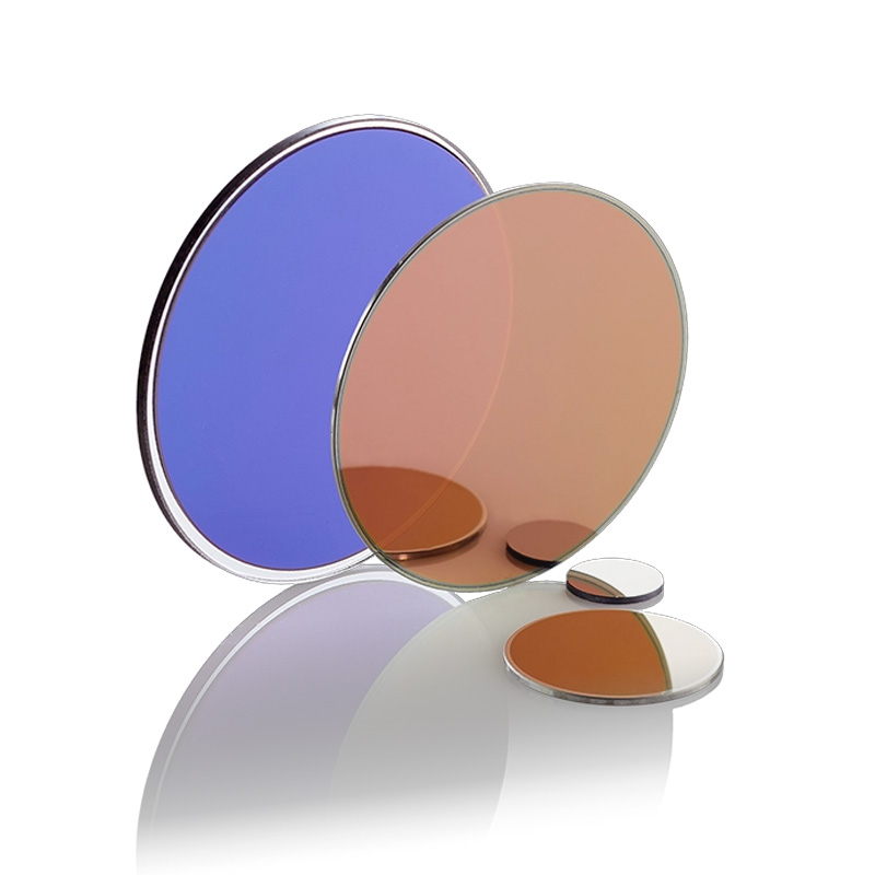
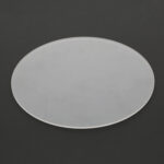
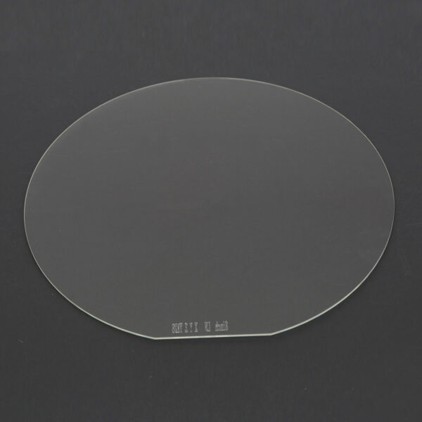
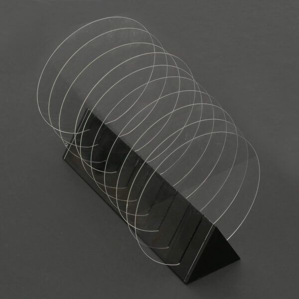
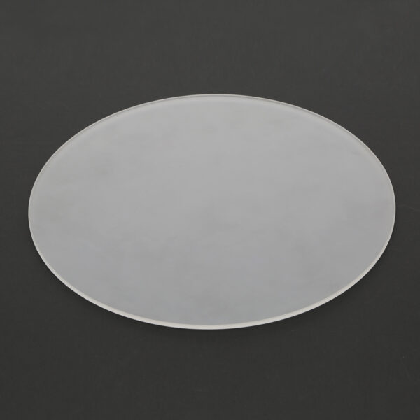
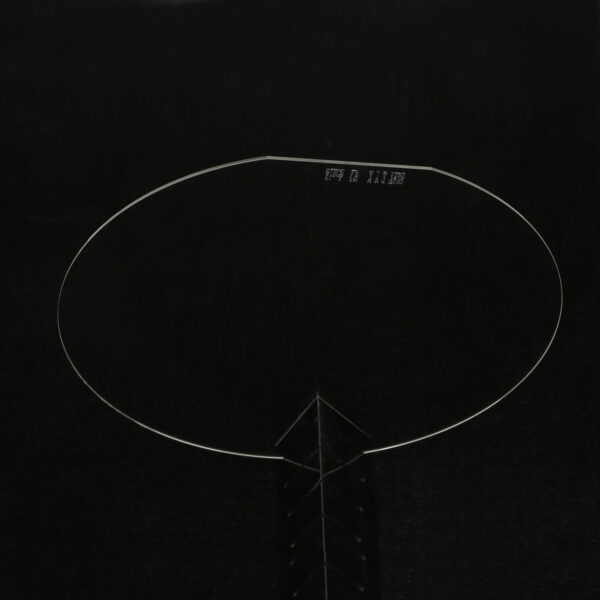
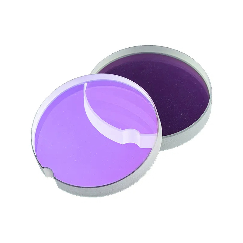
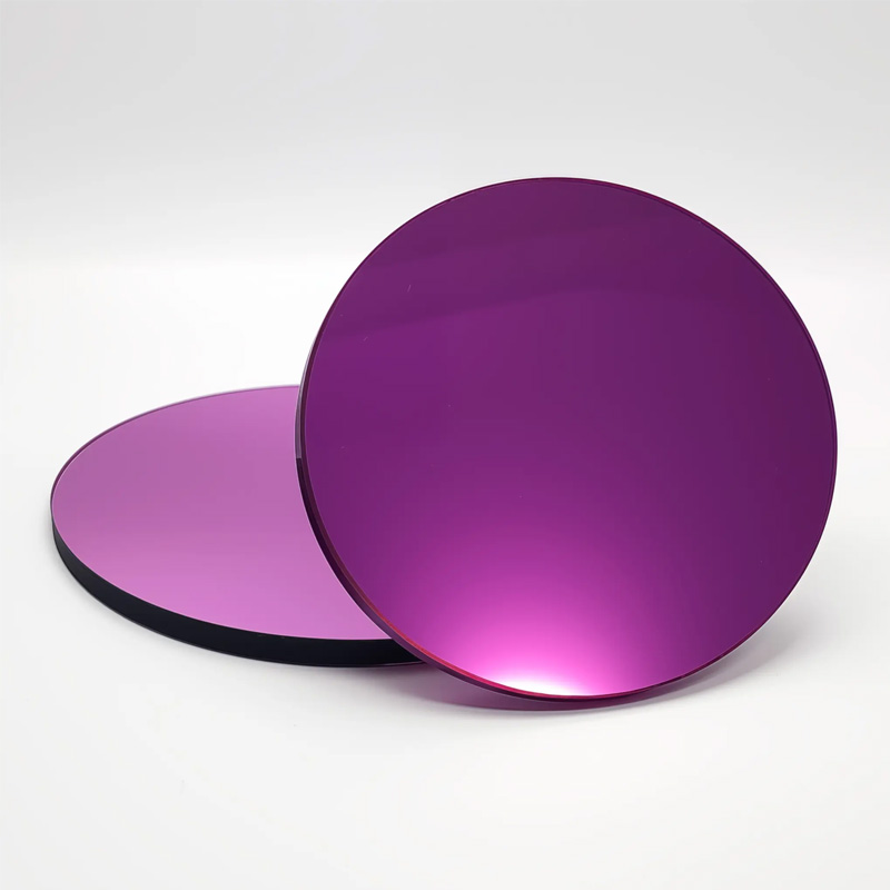
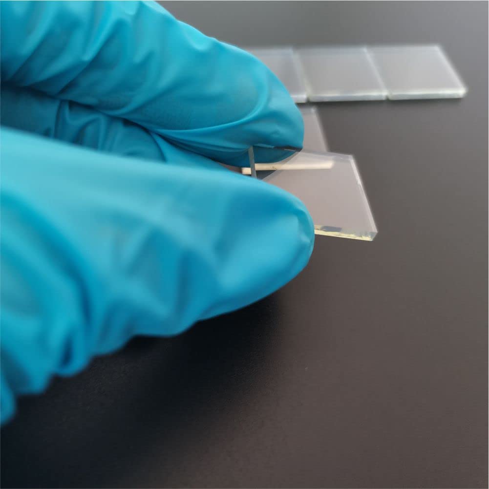
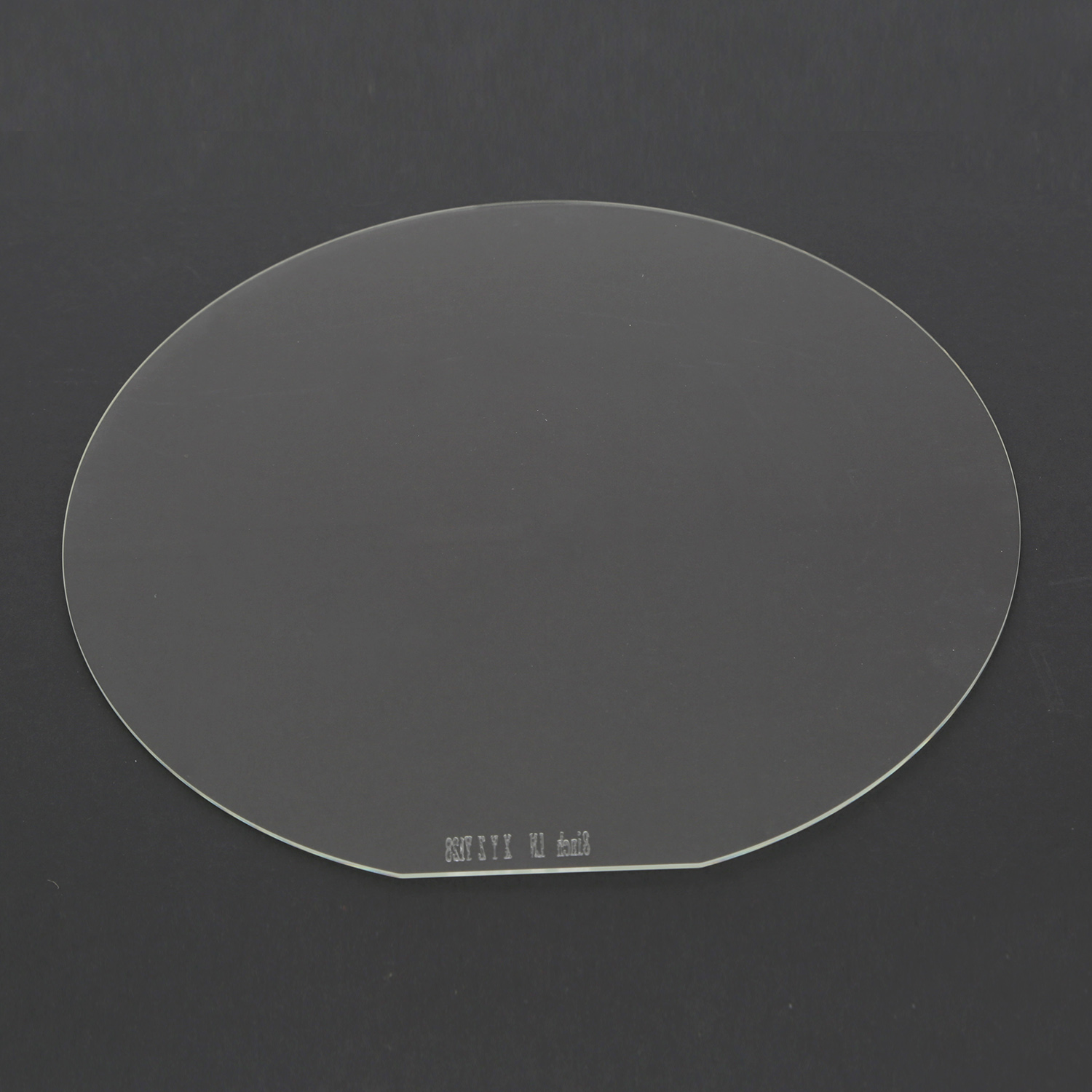
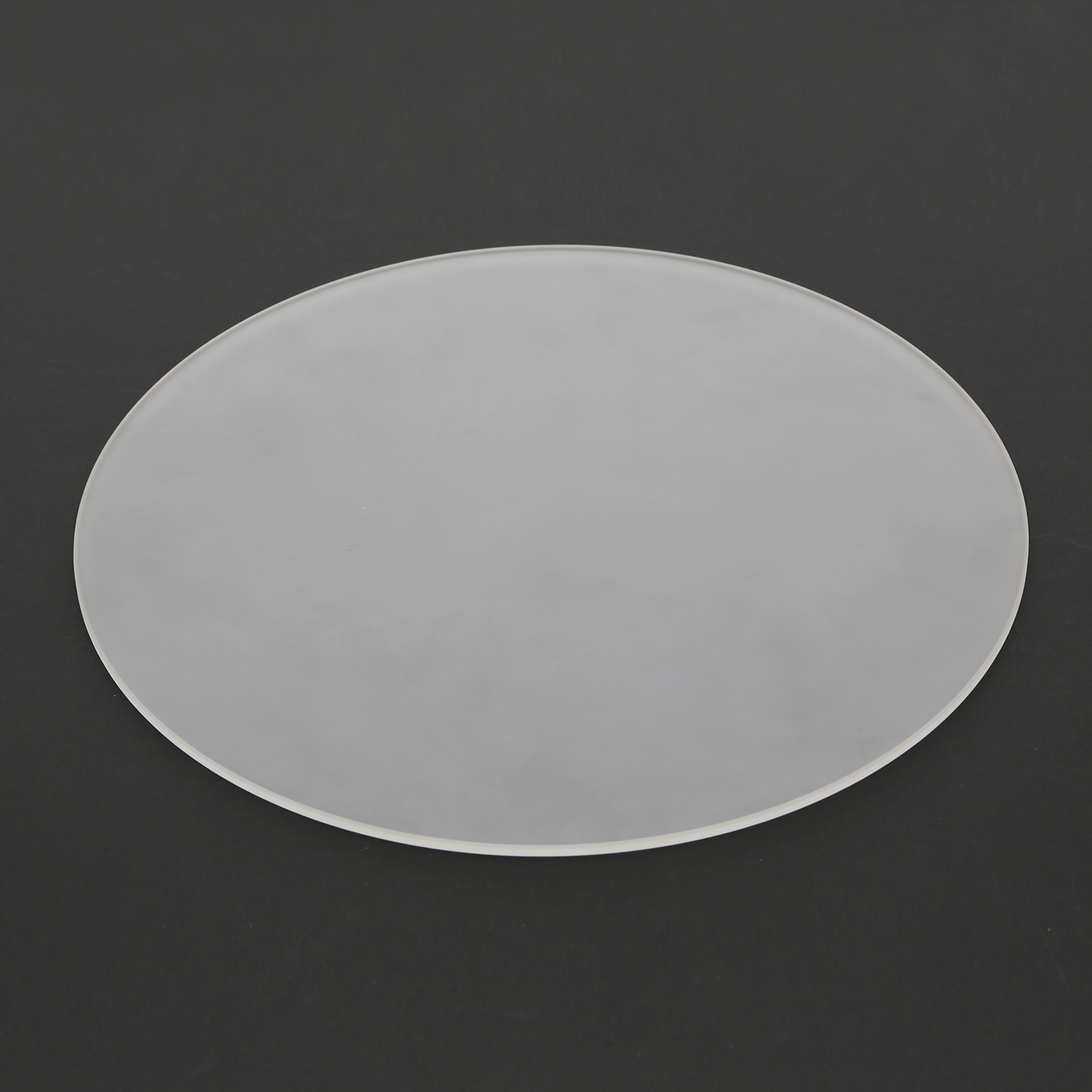
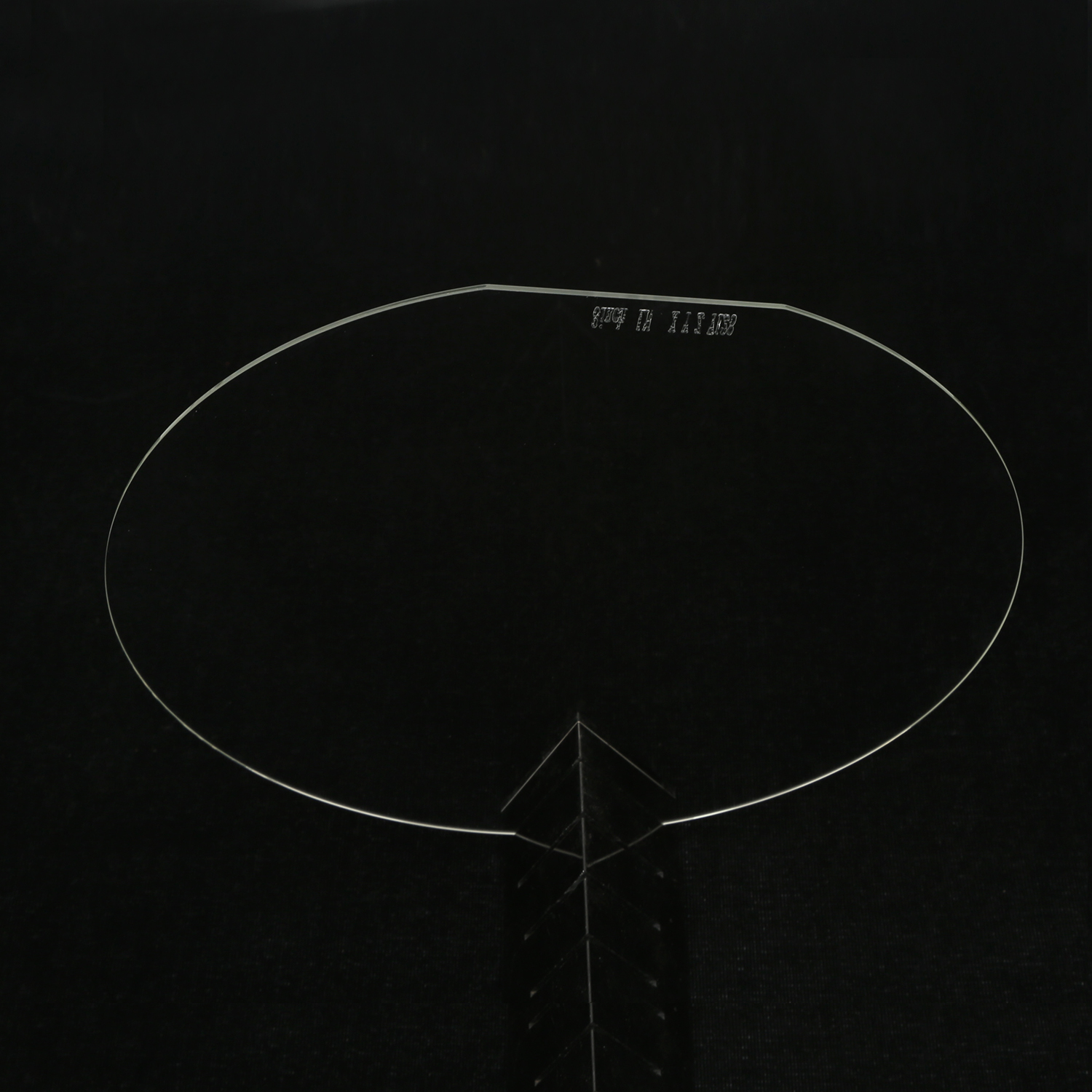
Fused silica glass wafers, also known as ultra-flat quartz wafers, are high-purity optical substrates made from amorphous silicon dioxide (SiO₂). Originally developed for semiconductor and photonic applications, these wafers offer exceptional UV transparency, thermal stability, and chemical resistance. Available in sizes from 2 to 12 inches, and thicknesses from 0.15 mm to 1.0 mm, they are widely used in MEMS, microfluidics, laser optics, and thin-film deposition. TIHOTOPTICS offers both JGS1 and JGS2 grade wafers with DSP or SSP finishes, customizable to your technical requirements.
Fused silica wafer technology continues to be the foundation of cutting-edge development in photonics, semiconductors, microfluidics, and bioengineering. With unmatched thermal stability, superior optical clarity, and ultra-low impurity levels, these high-precision substrates enable next-generation innovations in nanofabrication, MEMS design, and UV-optics.
At TIHOTOPTICS, we specialize in ultra-flat fused silica glass wafers ranging from 2” to 12” in diameter, precision-polished on one or both sides (SSP/DSP), and customizable in thickness from 150 µm to 1.0 mm. We offer JGS1 and JGS2 material grades, each optimized for specific spectral and performance requirements.
What Is a Fused Silica Wafer?
A fused silica wafer is a thin, ultra-flat disc made from high-purity amorphous silicon dioxide (SiO₂), typically formed via flame hydrolysis or electric fusion methods. The non-crystalline structure provides unique advantages including:
Outstanding thermal shock resistance
Minimal thermal expansion (0.55 × 10⁻⁶/°C)
Broadband transmission from UV (180 nm) to IR (2500 nm)
Low autofluorescence and birefringence
Exceptional chemical inertness and purity
These properties make fused silica wafers ideal for advanced processes such as photolithography, laser optics, microfluidics, MEMS fabrication, and bio-sensing.
Fused Silica Wafer Applications
Photolithography and Photomasks
Due to their excellent flatness and spectral transparency, fused silica wafers are widely used as photomask substrates in semiconductor manufacturing. The DSP surface finish ensures ultra-low roughness and perfect light transmission in deep-UV lithography (DUV) systems.
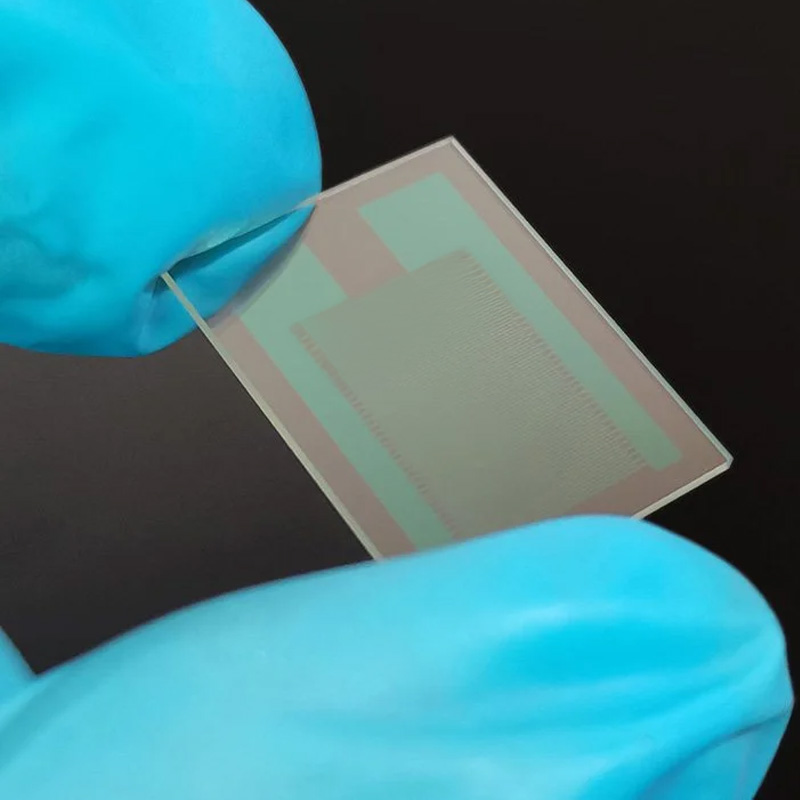
Microfluidics and MEMS Devices
The chemical resistance and optical clarity of fused silica make it a preferred substrate for microfluidic chip fabrication. These wafers support plasma bonding, laser drilling, and precise channel structuring critical in bio-diagnostic and environmental sensor applications.
UV/VUV Optical Components
JGS1 grade fused silica wafers offer maximum UV and VUV light transmission (180–250 nm), making them essential in spectroscopic systems, excimer lasers, and advanced optical coating platforms.
Thin Film Deposition and Testing
With an ultra-low Total Thickness Variation (TTV) and sub-nanometer roughness, these wafers provide an ideal base for thin film characterization, plasma-enhanced deposition, and refractive index testing.
Wafer-Level Packaging (WLP) and Optical Windows
Fused silica is used in WLP applications to provide sealing and transparency in optical MEMS, bio-MEMS, and LED packaging. Its thermal expansion match with silicon and robust mechanical properties ensure long-term reliability.
Grades of Fused Silica: JGS1 vs. JGS2
Property
JGS1
JGS2
UV Transmission
Superior (down to 180 nm)
Moderate (down to ~220 nm)
Visible Clarity
Excellent
Very Good
Thermal Stability
High
High
Common Use
Deep-UV optics, excimer lasers
General-purpose optics
JGS1 is preferred for DUV, laser optics, and lithography, whereas JGS2 offers a cost-effective solution for standard optical and microfabrication tasks.
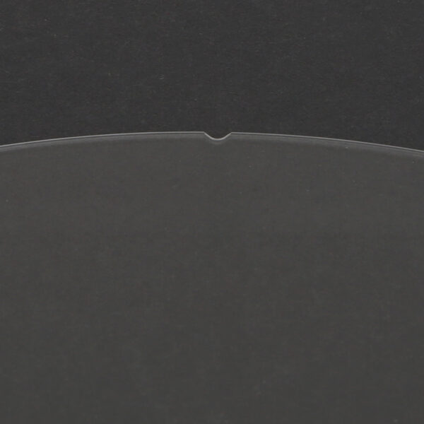
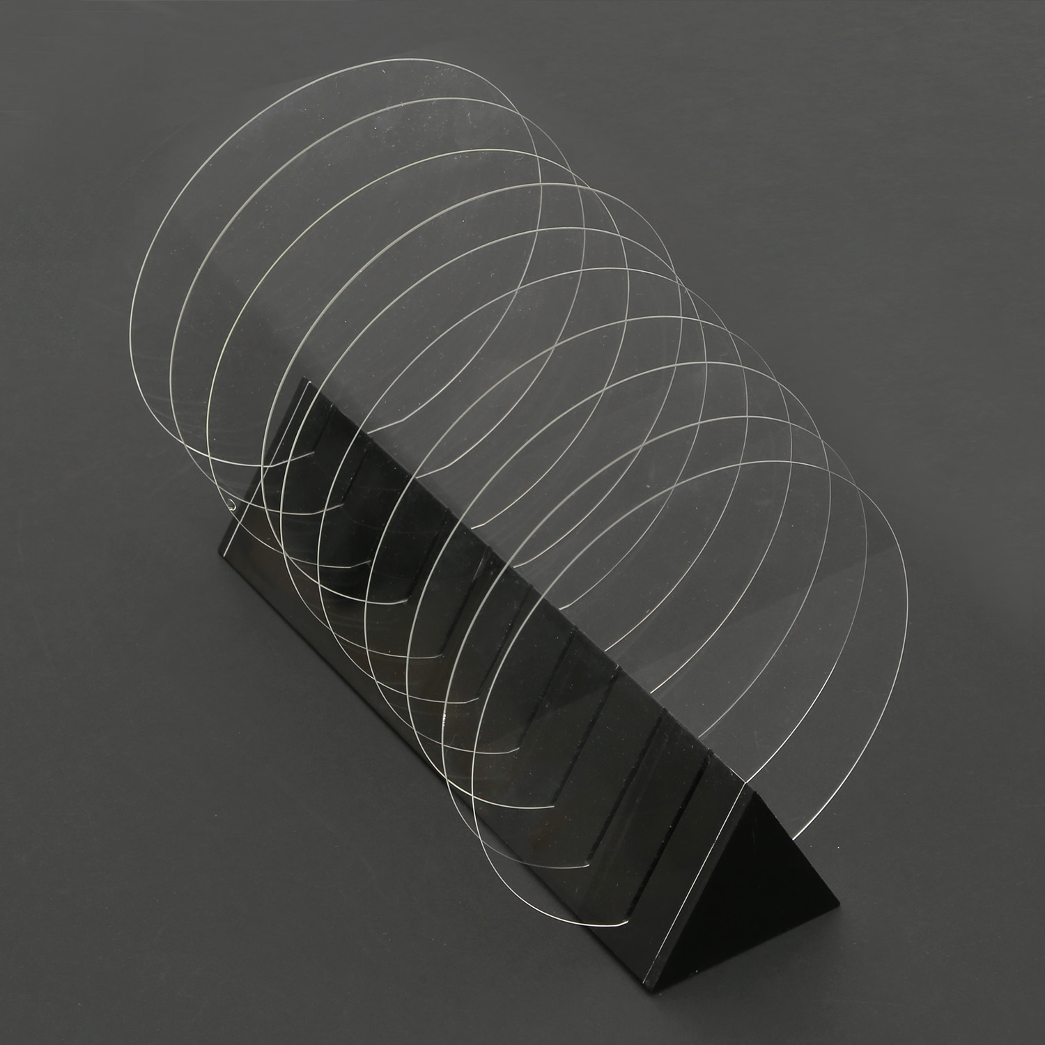
Advantages of Double-Side Polished Fused Silica Wafers
High parallelism essential for interference lithography and bonding processes
Ultra-low roughness (<1 nm Ra) enables maximum reflectivity and minimal scattering
Reduced bow and warp enhances film deposition uniformity and etching precision
Suitable for vacuum, cryogenic, or plasma environments
Custom Fused Silica Wafer Options
We offer fully customizable solutions tailored to your application. Options include:
Diameter sizes from 1” to 12”
Thicknesses from 150 µm to 1.0 mm
DSP/SSP surface finishes
TTV tolerances as low as <5 µm for extreme precision
Etched channels, holes, or edge modifications
Compatibility with plasma, chemical, and mechanical bonding techniques
Why Choose TIHOTOPTICS for Fused Silica Wafers?
ISO-quality manufacturing processes with cleanroom standards
Short lead times on standard and custom wafer builds
Expert support in optoelectronics, photonics, and microfluidics
Competitive pricing and full traceability on JGS1/JGS2 materials
Industry-grade metrology and inspection tools ensure defect-free wafers
People Also Ask
What is the difference between JGS1, JGS2, and JGS3?
JGS1: Maximum UV transparency, lowest impurities, best for DUV.
JGS2: Balanced UV-visible transmission, great for general optics.
JGS3: More economical, good for IR applications and non-critical optics.
Why is double-side polishing important?
DSP ensures ultra-flat, highly parallel surfaces ideal for wafer bonding, high-resolution lithography, and precise optical systems.
Can fused silica wafers withstand high temperatures?
Yes, they remain structurally stable at up to 1000°C and resist thermal cycling, crucial in semiconductor processing.
Are these wafers compatible with microfluidics or MEMS?
Absolutely. Their chemical resistance, optical clarity, and dimensional stability make them ideal for lab-on-chip, biosensors, and actuator platforms.
Do you support custom wafers or features?
Yes. We fabricate custom diameters, holes, etched structures, and flat edges to support specialized research or commercial applications.
Get High-Purity Fused Silica Wafers – Fast & Reliable
Whether you’re working in nanophotonics, semiconductor R&D, life sciences, or advanced metrology, our fused silica wafer solutions deliver unmatched reliability, precision, and optical performance. TIHOTOPTICS is your trusted partner for consistent quality and technical expertise in optical substrate manufacturing.
Request a quote today and discover how our JGS1/JGS2 fused silica wafers can meet your most demanding project requirements.
Technical Specifications of Fused Silica Wafers (2”–12”)
Diameter
Size (mm)
Thickness Range (µm)
Surface Finish
TTV (µm)
Bow/Warp (µm)
Roughness (Ra)
Scratch-Dig
2″
50.8
150 – 1000
SSP / DSP
<8
<30
<1 nm
40/20
3″
76.2
150 – 1000
SSP / DSP
<10
<30
<1 nm
40/20
4″
100
150 – 1000
SSP / DSP
<10
<40
<1 nm
40/20
5″
125
150 – 1000
SSP / DSP
<10
<40
<1 nm
40/20
6″
150
150 – 1000
SSP / DSP
<15
<60
<1 nm
40/20
8″
200
150 – 1000
SSP / DSP
<20
<60
<1 nm
40/20
12″
300
On request
SSP / DSP
Custom
Custom
<1 nm
40/20
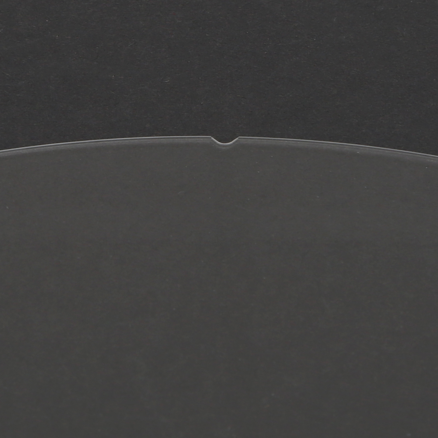
Custom options include alignment flats, edge bevels, center holes, and through-holes for alignment and bonding.
