

In precision optics, glass flatness is one of the most critical surface specifications. It defines how closely a glass surface matches a perfectly flat plane, directly influencing laser alignment, interferometric accuracy, and imaging quality. Even the most advanced optical glass isn’t truly flat—under microscopic inspection, subtle surface variations of just nanometers can significantly impact optical performance.
Think of it this way: if you could magnify a seemingly flat piece of optical glass to enormous proportions, you’d see a landscape of microscopic hills and valleys. These variations might measure just a few nanometers (billionths of a meter), but in precision optics, even these tiny imperfections can significantly affect performance.
These minute deviations might seem insignificant, but in high-precision optical systems used in semiconductor manufacturing, metrology, and laser optics, they can introduce phase errors, distort images, and reduce measurement accuracy. Understanding and controlling flatness is essential for achieving optimal optical performance.
Why Glass Flatness Matters in Optical Applications
In optical systems, the performance of light transmission and reflection depends heavily on surface precision. When a glass substrate or wafer surface deviates from perfect flatness, the wavefront of light becomes distorted, leading to optical aberrations, phase errors, and reduced coherence. Even nanometer-scale deviations can compromise the accuracy and stability of precision instruments.
Real-World Impacts of Poor Flatness
Imaging and Optical Systems: Uneven surfaces introduce focus shifts and distortions, degrading image contrast and resolution.
Laser Mirrors: Surface irregularities scatter or diffuse light, lowering reflectivity and reducing output power.
Semiconductor Wafers: Variations in thickness or planarity affect photolithography alignment and device layer uniformity.
Understanding Key Glass Flatness Parameters
Glass flatness isn’t measured by a single number. Instead, optical engineers evaluate it through several interrelated parameters that together provide a complete picture of surface quality and geometric precision.
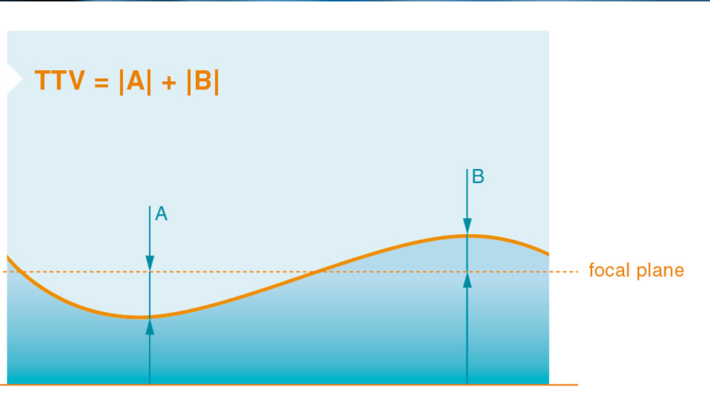
1. Total Thickness Variation (TTV)
Definition:
TTV measures the maximum thickness difference across a glass surface—specifically, the distance between the thickest and thinnest points of the substrate.
Why TTV Matters:
Low TTV ensures uniform glass thickness, which is crucial for:
- Consistent light transmission through the material
- Minimizing optical path length distortion
- Maintaining precise focus in imaging systems
- Achieving high parallelism in optical windows
Industry Standards:
| Application Type | Typical TTV Range | Use Case |
|---|---|---|
| High-precision optical substrates | ≤ 0.5–1 μm | Laser optics, interferometry |
| Standard optical windows | ≤ 2–3 μm | General imaging systems |
| Industrial glass components | ≤ 5–10 μm | Non-critical optical applications |
Technical Note: For thin wafers or precision optics, even a few micrometers of thickness variation can affect focus calibration and system performance.
2. Surface Figure Error
Definition:
Surface Figure Error quantifies how much the actual glass surface deviates from its ideal flat geometry. This deviation is typically expressed as a fraction of the test wavelength, such as λ/4, λ/10, or λ/20 (where λ is usually the He-Ne laser wavelength of 632.8 nm).
Why Surface Figure Matters:
These deviations directly alter the reflected or transmitted wavefront, leading to:
- Phase errors in interferometric measurements
- Optical aberrations that degrade image quality
- Reduced coherence in laser applications
Measurement Approach:
Surface figure errors are measured using interferometry, where interference patterns reveal surface deviations with nanometer-scale accuracy. This non-contact method provides detailed surface maps showing exactly where and how much deviation exists.
Common Specifications:
| Optical Grade | Surface Figure | Application |
|---|---|---|
| Precision grade | λ/20 or better | Laser mirrors, reference flats |
| Standard grade | λ/10 to λ/4 | General optical windows |
| Commercial grade | λ/4 to λ/2 | Non-critical viewing optics |
3. Peak-to-Valley (PV) Flatness
Definition:
PV (Peak-to-Valley) represents the maximum vertical distance between the highest peak and lowest valley on a surface. It’s the most straightforward flatness metric—literally the maximum height difference across the entire glass surface.
Practical Example:
A surface flatness specification of λ/10 PV means that across the entire glass, the maximum height variation equals one-tenth of the test wavelength. Using a He-Ne laser (632.8 nm):
- λ/10 = 63.3 nm maximum deviation
- λ/20 = 31.6 nm maximum deviation
Advantages and Limitations:
- Simple to understand and directly interpretable
- Shows worst-case surface deviation
- Only captures extremes—doesn’t reflect overall surface uniformity
- Should be paired with RMS for complete assessment
Typical PV Requirements:
| Application | PV Specification | Precision Level |
|---|---|---|
| Reference optical flats | λ/20 to λ/40 | Ultra-high precision |
| Laser-grade optics | λ/10 to λ/20 | High precision |
| Standard optical windows | λ/4 to λ/10 | Medium precision |
| General use glass | λ/2 or greater | Standard quality |
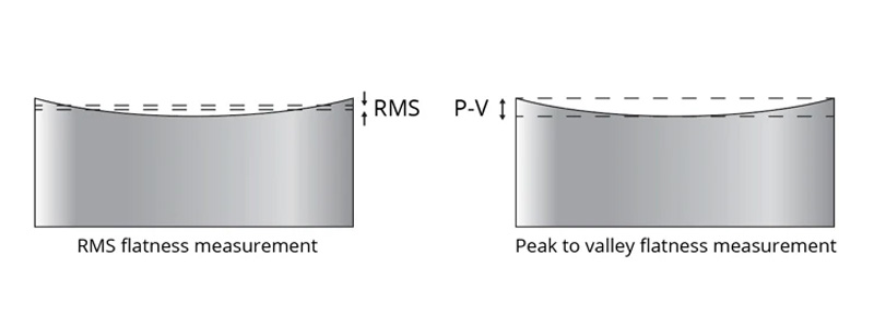
4. Root Mean Square (RMS) Flatness
Definition:
RMS (Root Mean Square) flatness represents the statistical average of all surface height deviations across the entire surface. Unlike PV, which only considers extreme points, RMS accounts for every measurement point, providing insight into overall surface smoothness.
Why RMS Is Important:
RMS provides a more accurate representation of how the surface will affect optical performance:
- Better correlation with actual wavefront quality
- More sensitive to overall surface uniformity
- Less affected by isolated defects or edge effects
Mathematical Relationship:
For most optical surfaces, RMS ≈ PV/3 to PV/5, though this ratio varies depending on surface profile characteristics.
In Practice:
RMS is especially critical for:
- Metrology-grade optical flats used as measurement references
- Laser-grade mirrors requiring excellent wavefront preservation
- High-NA imaging systems sensitive to phase errors
Quality Comparison:
| Surface Quality | PV Specification | RMS Specification | Application |
|---|---|---|---|
| Ultra-precision | λ/20 | λ/100 | Interferometer references |
| High precision | λ/10 | λ/50 | Laser optics |
| Standard precision | λ/4 | λ/20 | Optical windows |
How Glass Flatness Is Achieved
Attaining ultra-flat glass surfaces requires advanced manufacturing processes, precision measurement, and careful quality control.
Manufacturing Processes:
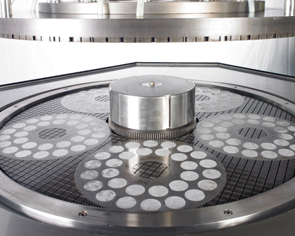
Double-Sided Lapping and Polishing
- Ensures uniform thickness across the substrate
- Removes material simultaneously from both surfaces
- Critical for achieving low TTV values
Precision Polishing
- Uses fine abrasives and controlled pressure
- Achieves surface roughness below 1 nm Ra
- Enables flatness specifications of λ/20 or better
Thermal Annealing
- Removes internal stresses that cause warping
- Stabilizes the glass structure
- Prevents post-processing deformation
Interferometric Testing
- Maps surface deviations with nanometer precision
- Provides real-time feedback during manufacturing
- Enables closed-loop process control
Applications Requiring High Glass Flatness
1. Laser Optics
Laser mirrors, beam splitters, and optical windows require excellent flatness to maintain beam quality and prevent wavefront distortion.
2. Interferometry
Reference flats and substrate mirrors in interferometers need λ/20 flatness or better to ensure accurate measurements.
3. Semiconductor Manufacturing
Silicon wafers and photomask substrates require tight TTV control for precise photolithography alignment.
4. Precision Metrology
Optical flats used as measurement standards demand ultra-high flatness for calibration accuracy.
5. Imaging Systems
High-resolution cameras and telescopes benefit from flat optical windows that don’t introduce aberrations.
Frequently Asked Questions (FAQ)
Q: What does λ/10 flatness mean?
A: It means the maximum surface deviation (PV) is one-tenth of the test wavelength, typically 63.3 nm when using a 632.8 nm He-Ne laser.
Q: Is PV or RMS more important?
A: Both are important. PV shows worst-case deviation, while RMS better represents overall optical performance. Use both for complete assessment.
Q: How is glass flatness measured?
A: Primarily through interferometry, which uses light interference patterns to map surface deviations with nanometer precision.
Q: What’s the difference between flatness and parallelism?
A: Flatness measures deviation from a perfect plane on one surface. Parallelism measures the angle between two opposite surfaces.
Q: Can flatness degrade over time?
A: High-quality optical glass maintains flatness unless subjected to thermal stress, mechanical damage, or improper storage conditions.